描述
产品简要说明
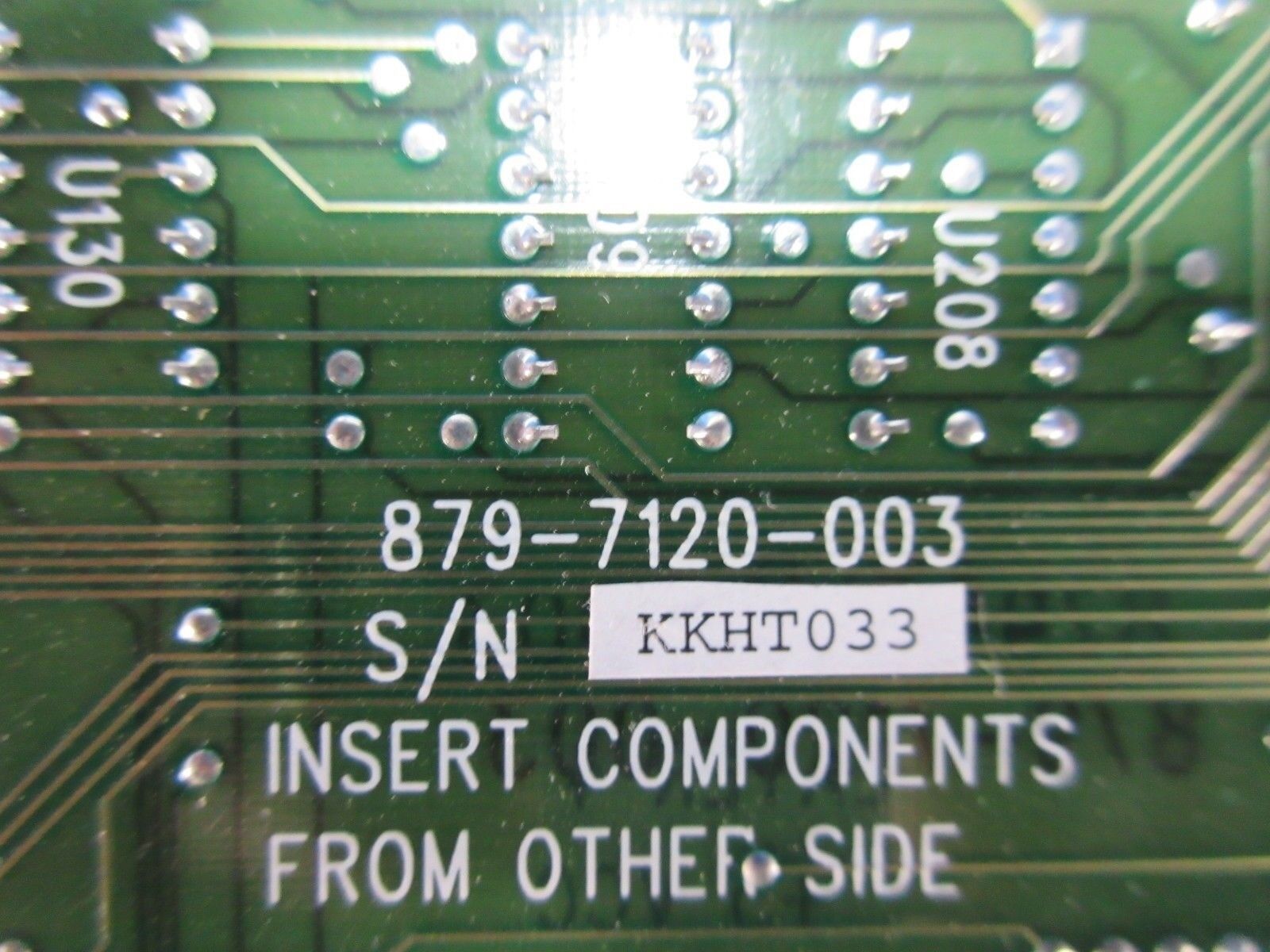
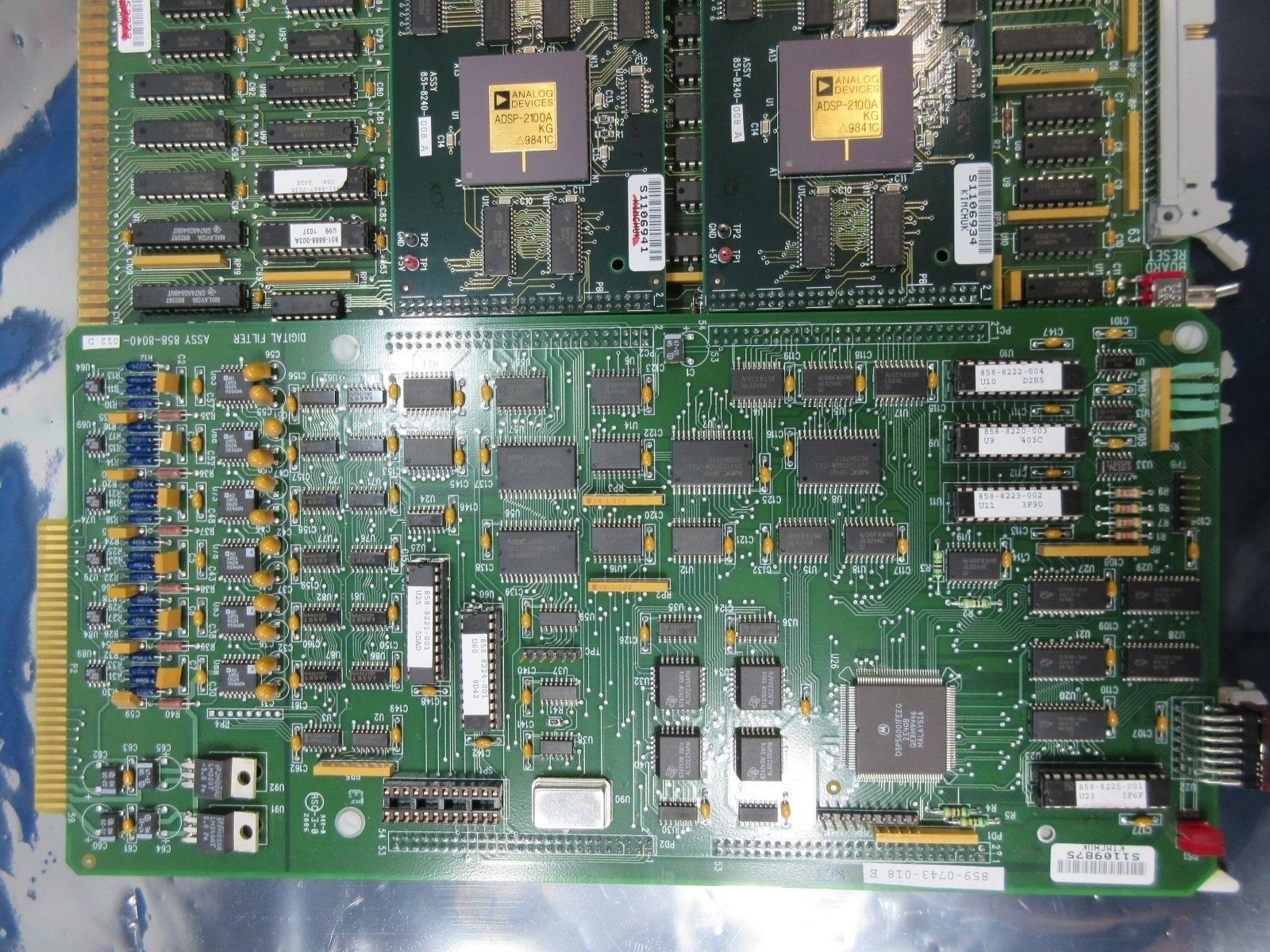
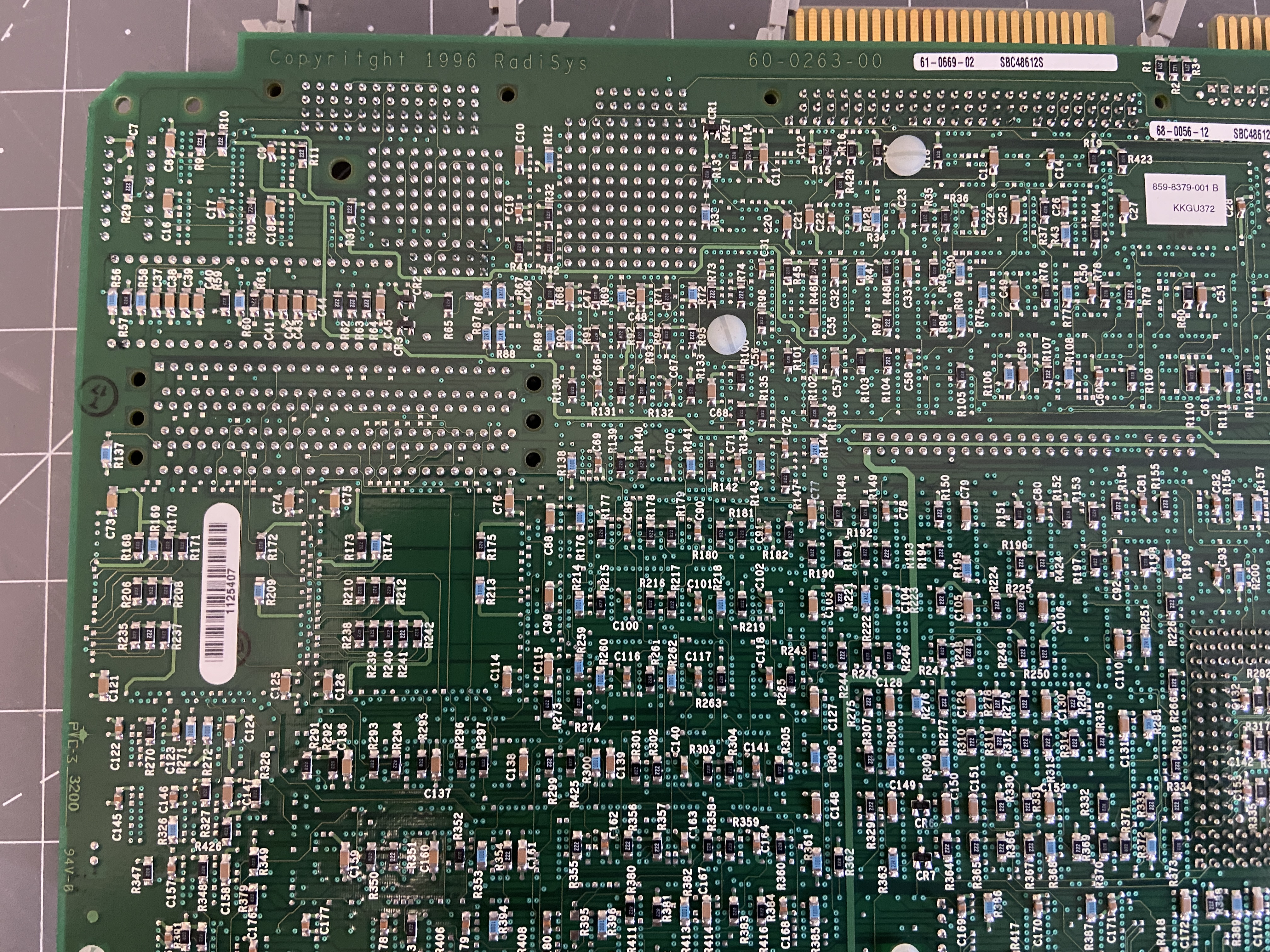
ASML 859-0743-018E是ASML专为极紫外(EUV)光刻机研发的高密度多层印刷电路板(PCB),核心特性包括:
12层叠层设计:支持GHz级高频信号传输与纳米级精度控制。
定制化适配:适配光刻机曝光控制、掩模台定位及晶圆检测系统。
工业级可靠性:通过Class 1洁净室认证,满足24/7连续运行需求。
产品详细说明
1.技术架构与核心功能
多层精密叠层:
采用高导热复合基材(FR4与聚酰亚胺混合结构),支持12层电路堆叠,减少信号串扰。
内置独立电源层与地层,优化电源分配效率,EMI抑制能力达40dB。
高频信号处理:
支持10GHz高频信号传输,插入损耗≤0.3dB,满足EUV光源控制需求。
集成阻抗匹配模块与滤波器,信号完整性(S参数)误差<±2%。
定制化布局:
支持异形尺寸(如曲面或镂空结构),适配光刻机紧凑化布局。
提供标准化接口(如PCIe 5.0)与定制化连接器(高密度FPC柔性接口)。
2.性能优势
高可靠性:
通过-40℃~125℃温度循环测试,热膨胀系数(CTE)与光刻机基材匹配。
抗湿性等级IP67,适应洁净室高纯度气体环境。
能效优化:
动态电源管理技术,待机功耗≤2W,整体能效提升30%。
抗干扰设计:
层间屏蔽层与接地隔离设计,EMC等级Class B(10V/m辐射抗扰)。
3.行业适配性
半导体制造:
用于EUV光刻机曝光控制单元、掩模台定位及晶圆缺陷检测系统。
支持5nm及以下制程的纳米级精度控制需求。
工业自动化:
适配高精度运动控制卡、传感器网络等场景的高速数据传输需求。
技术规格:ASML 859-0743-018E
参数项规格描述
层数12层高密度叠层
基材类型FR4与聚酰亚胺复合材料
信号传输频率10GHz(插入损耗≤0.3dB)
尺寸范围定制化(最小尺寸:50mm×50mm)
工作温度-40℃~125℃
抗湿等级IP67(48小时浸水测试)
功耗≤15W(典型值)

Product brief description
ASML 859-0743-018E is a high-density multi-layer printed circuit board(PCB)developed by ASML for extreme ultraviolet(EUV)lithography machines.The core features include:
12-layer stacking design:supports GHz-level high-frequency signal transmission and nano-level accuracy control.
Customized adaptation:adapted to lithography machine exposure control,mask table positioning and wafer detection system.
Industrial-grade reliability:passed Class 1 clean room certification to meet the needs of 24/7 continuous operation.
Product details
1.Technical architecture and core functions
Multi-layer precision stacking:
It adopts a highly thermally conductive composite substrate(FR4 and polyimide mixed structure),supports 12-layer circuit stacking to reduce signal crosstalk.
Built-in independent power layer and formation,optimize power distribution efficiency,and EMI suppression capacity reaches 40dB.
High frequency signal processing:
Supports 10GHz high-frequency signal transmission,insertion loss is≤0.3dB,meeting the EUV light source control needs.
Integrated impedance matching module and filter,signal integrity(S parameter)error<±2%.
Customized layout:
Supports special-shaped sizes(such as curved surfaces or hollow structures),and is suitable for compact layout of lithography machines.
Provides standardized interfaces(such as PCIe 5.0)and customized connectors(high-density FPC flexible interface).
2.Performance Advantages
High reliability:
Through the temperature cycle test of-40℃~125℃,the thermal expansion coefficient(CTE)matches the substrate of the lithography machine.
Wet resistance level IP67,adapts to high-purity gas environment in clean rooms.
Energy efficiency optimization:
Dynamic power management technology,standby power consumption≤2W,and overall energy efficiency is improved by 30%.
Anti-interference design:
Design of interlayer shielding and ground isolation,EMC grade Class B(10V/m radiation immunity).
3.Industry adaptability
Semiconductor manufacturing:
It is used in the exposure control unit of EUV lithography machine,mask table positioning and wafer defect detection system.
Supports nano-level precision control requirements for processes with 5nm and below.
Industrial automation:
It is suitable for high-speed data transmission requirements in scenarios such as high-precision motion control cards,sensor networks,etc.
Technical Specifications:ASML 859-0743-018E
Parameters Specification Description
Number of layers 12 high-density stacks
Substrate type FR4 and polyimide composite material
Signal transmission frequency:10GHz(insert loss≤0.3dB)
Size range Customized(minimum size:50mm×50mm)
Working temperature-40℃~125℃
Wet resistance grade IP67(48-hour water immersion test)
Power consumption≤15W(typical)


