描述
产品简要说明
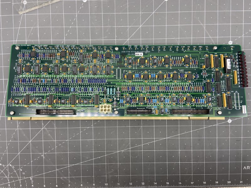
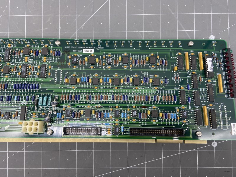
ASML 859-0929-006是ASML专为极紫外(EUV)光刻机设计的高精度光学检测传感器,核心功能包括:
纳米级光强监测:实时检测曝光能量波动,精度达±0.005%(单脉冲)。
动态反馈控制:与光刻机控制系统联动,曝光均匀性误差<0.2%。
多模态数据采集:集成光谱分析、偏振检测与温度补偿模块,适配复杂工艺需求。
产品详细说明
1.技术架构与核心功能
光学检测系统:
超快响应探测器:采用硅光电倍增管(SiPM)阵列,响应时间≤50ps,覆盖13.5nm EUV波段。
多通道数据处理:支持8路并行信号采集,采样率100MHz,动态范围10^6:1。
补偿算法:
温度自适应校准:通过热电堆传感器实时监测环境温度,补偿因热漂移导致的光强误差。
光路损耗补偿:结合ASML的Source Mask Optimization(SMO)算法,动态调整曝光能量分布。
抗干扰设计:
电磁屏蔽:三层屏蔽结构(含氮化钛涂层),抑制外部电磁干扰至<0.01V/m。
机械稳定性:气浮轴承支撑系统,振动敏感度≤0.1nm/rms(0.1Hz~1kHz)。
2.性能突破
制程兼容性:
支持3nm及以下逻辑芯片与2nm存储芯片的曝光监控需求。
能效优化:
功耗≤25W(典型值),较上代降低40%,热辐射影响减少至0.01℃/W。
故障自诊断:
内置AI算法(基于LSTM网络),可检测传感器老化与污染,误报率<0.05%。
3.行业适配性
半导体制造:
用于EUV光源能量校准、掩模版缺陷检测及晶圆曝光实时监控。
适配先进封装(如Chiplet异构集成)的微米级能量均匀性需求。
科研领域:
支持量子点阵列、纳米光子器件的高精度光强测量与分析。
技术规格:ASML 859-0929-006
参数项规格描述
检测波长13.5nm(EUV波段)
精度±0.005%(单脉冲能量波动)
响应时间≤50ps(上升沿)
采样率100MHz(8通道并行)
环境适应性温度范围:10℃~35℃,湿度≤5%RH(非凝露)
功耗≤25W(典型值)
Product brief description
ASML 859-0929-006 is a high-precision optical detection sensor designed by ASML for extreme ultraviolet(EUV)lithography machines.The core functions include:
Nano-level light intensity monitoring:detect exposure energy fluctuations in real time,with an accuracy of±0.005%(single pulse).
Dynamic feedback control:linked to the lithography machine control system,exposure uniformity error is<0.2%.
Multimodal data acquisition:Integrated spectral analysis,polarization detection and temperature compensation modules to adapt to complex process requirements.
Product details
1.Technical architecture and core functions
Optical detection system:
Ultrafast response detector:adopts silicon photomultiplier tube(SiPM)array,with a response time≤50ps,covering the 13.5nm EUV band.
Multi-channel data processing:supports 8-channel parallel signal acquisition,sampling rate 100MHz,dynamic range 10^6:1.
Compensation algorithm:
Temperature adaptive calibration:The ambient temperature is monitored in real time through the thermopile sensor to compensate for the light intensity error caused by thermal drift.
Optical path loss compensation:combined with ASML’s Source Mask Optimization(SMO)algorithm,dynamically adjust the exposure energy distribution.
Anti-interference design:
Electromagnetic shielding:three-layer shielding structure(including titanium nitride coating),inhibiting external electromagnetic interference to<0.01V/m.
Mechanical stability:air-floating bearing support system,vibration sensitivity≤0.1nm/rms(0.1Hz~1kHz).
2.Performance breakthrough
Process compatibility:
Supports exposure monitoring requirements for logic chips below 3nm and below and 2nm memory chips.
Energy efficiency optimization:
Power consumption is≤25W(typical),40%lower than the previous generation,and the influence of thermal radiation is reduced to 0.01℃/W.
Self-diagnosis of faults:
Built-in AI algorithm(based on LSTM network)can detect sensor aging and pollution,with a false alarm rate<0.05%.
3.Industry adaptability
Semiconductor manufacturing:
Used for EUV light source energy calibration,mask defect detection and wafer exposure real-time monitoring.
Adapt micron-scale energy uniformity requirements in advanced packaging such as Chiplet heterogeneous integration.
Scientific research fields:
Supports high-precision light intensity measurement and analysis of quantum dot arrays and nanophoton devices.
Technical Specifications:ASML 859-0929-006
Parameters Specification Description
Detection wavelength:13.5nm(EUV band)
Accuracy±0.005%(single pulse energy fluctuation)
Response time≤50ps(rise edge)
Sample rate:100MHz(8 channels parallel)
Environmental adaptability Temperature range:10℃~35℃,humidity≤5%RH(non-condensing)
Power consumption≤25W(typical)