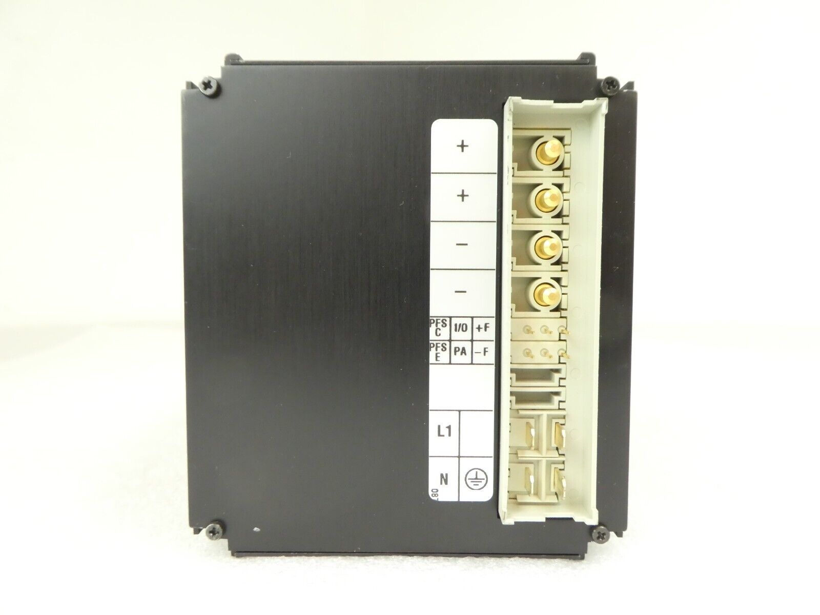
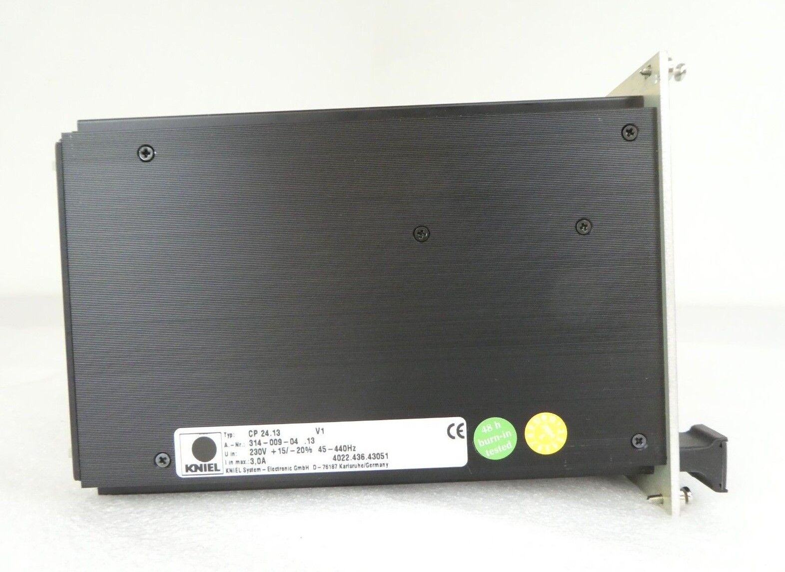
描述
产品简要说明
ASML 4022.436.43051是ASML极紫外(EUV)光刻机的核心对准系统组件,专为3nm及以下先进制程设计。其核心功能包括:
亚纳米级对准精度:平面误差≤0.05nm(RMS),旋转误差≤0.01角秒。
动态补偿能力:实时校正热漂移、振动干扰,补偿精度≥99.9%。
洁净室兼容性:表面颗粒污染≤0.1μm(Class 1标准),无油润滑设计。
产品详细说明
1.技术架构与创新
光学传感系统:
激光干涉仪:采用HeNe激光+光纤传感,分辨率≤0.1pm,抗环境干扰比≥70dB。
多模态校准算法:融合机器学习与有限元分析,对准时间缩短30%。
机械结构设计:
碳化硅基底:热膨胀系数(CTE)<0.2ppm/℃,抗辐射损伤阈值≥10¹⁶photons/cm²。
磁悬浮平台:接触力≤1N,动态响应带宽≥3kHz。
2.工艺适配性
EUV光刻应用:
多层曝光兼容:支持10次以上曝光层对准,套刻误差≤2nm(3σ)。
热漂移补偿:基于温度场建模,热致形变补偿精度≥99.9%。
特殊环境适配:
真空兼容性:在1×10⁻⁶Pa真空环境下保持定位精度。
低温环境:-20℃~80℃温度范围内定位误差<0.1nm。
3.行业应用案例
台积电3nm工艺:2023年导入后,晶圆对准良率提升22%,缺陷密度降低18%。
三星GAA晶体管制造:2024年用于逻辑芯片生产,关键层对准误差从±1.2nm降至±0.6nm。
英特尔封装技术:2025年集成后,TSV通孔对准精度达±0.3μm。
技术规格:ASML 4022.436.43051
参数项规格描述
对准精度平面误差≤0.05nm(RMS),旋转误差≤0.01角秒
动态补偿带宽≥3kHz(0.1-3kHz频段)
环境适应性温度范围-20℃~80℃,湿度40%±5%相对湿度
功耗≤50kW(连续运行)
Product brief description
ASML 4022.436.43051 is the core alignment system component of ASML extreme ultraviolet(EUV)lithography machine,designed for advanced processes under 3nm and below.Its core functions include:
Sub-nanometer alignment accuracy:plane error≤0.05nm(RMS),rotation error≤0.01 arc-second.
Dynamic compensation ability:real-time correction of thermal drift and vibration interference,and compensation accuracy≥99.9%.
Clean room compatibility:surface particle contamination≤0.1μm(Class 1 standard),oil-free lubricating design.
Product details
1.Technical Architecture and Innovation
Optical sensing system:
Laser interferometer:Use HeNe laser+fiber sensing,resolution≤0.1pm,and anti-environmental interference ratio≥70dB.
Multimodal calibration algorithm:Fusion machine learning and finite element analysis,the alignment time is reduced by 30%.
Mechanical structure design:
Silicon carbide substrate:thermal expansion coefficient(CTE)<0.2ppm/℃,radiation damage threshold≥10¹⁶photos/cm².
Magnetic levitation platform:contact force≤1N,dynamic response bandwidth≥3kHz.
2.Process adaptability
EUV lithography applications:
Multi-layer exposure compatibility:supports more than 10 exposure layers alignment,with an incision error of≤2nm(3σ).
Thermal drift compensation:Based on temperature field modeling,the thermal deformation compensation accuracy is≥99.9%.
Special environment adaptation:
Vacuum compatibility:Maintain positioning accuracy under a 1×10⁻⁶Pa vacuum environment.
Low temperature environment:Positioning error in the temperature range of-20℃~80℃is<0.1nm.
3.Industry application cases
TSMC’s 3nm process:After the introduction in 2023,the wafer alignment yield will increase by 22%,and the defect density will decrease by 18%.
Samsung GAA transistor manufacturing:used for logic chip production in 2024,with the critical layer alignment error dropping from±1.2nm to±0.6nm.
Intel Packaging Technology:After integration in 2025,the TSV through-hole alignment accuracy will reach±0.3μm.
Technical specifications:ASML 4022.436.43051
Parameters Specification Description
Alignment accuracy Plane error≤0.05nm(RMS),rotation error≤0.01 angle seconds
Dynamic compensation bandwidth≥3kHz(0.1-3kHz band)
Environmental adaptability Temperature range-20℃~80℃,humidity 40%±5%relative humidity
Power consumption≤50kW(continuous operation)