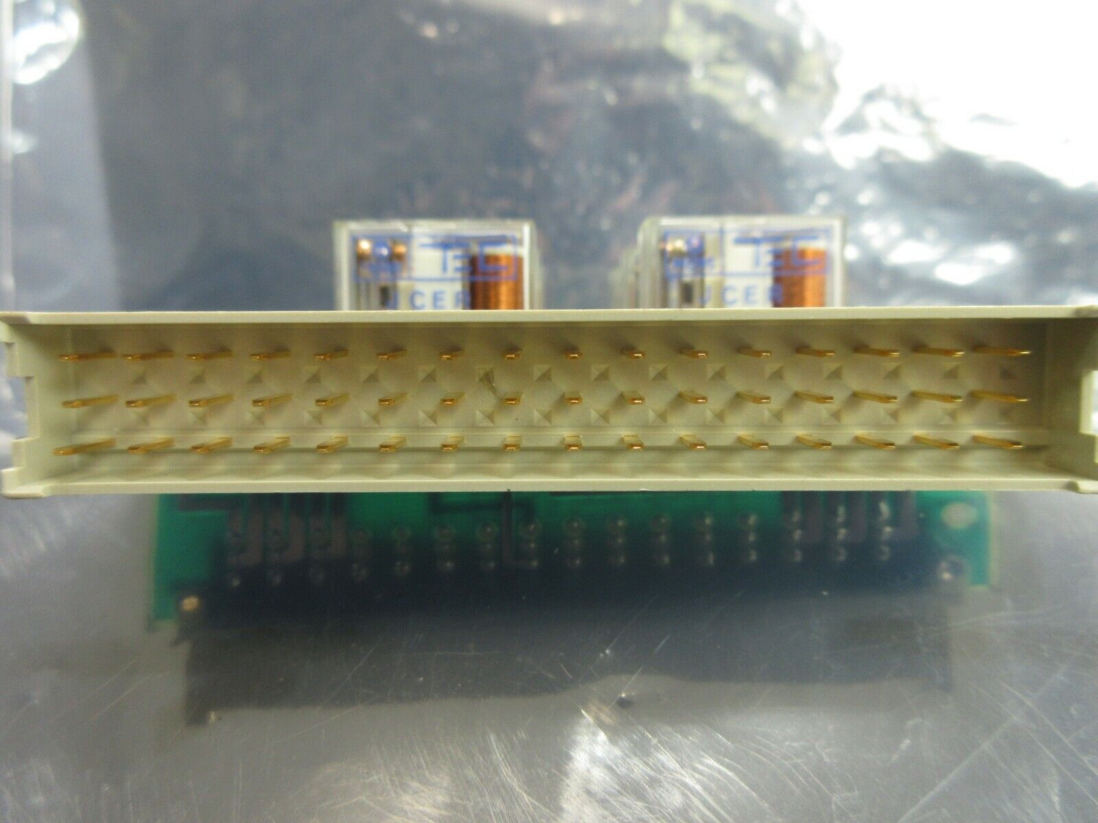
描述
产品简要说明
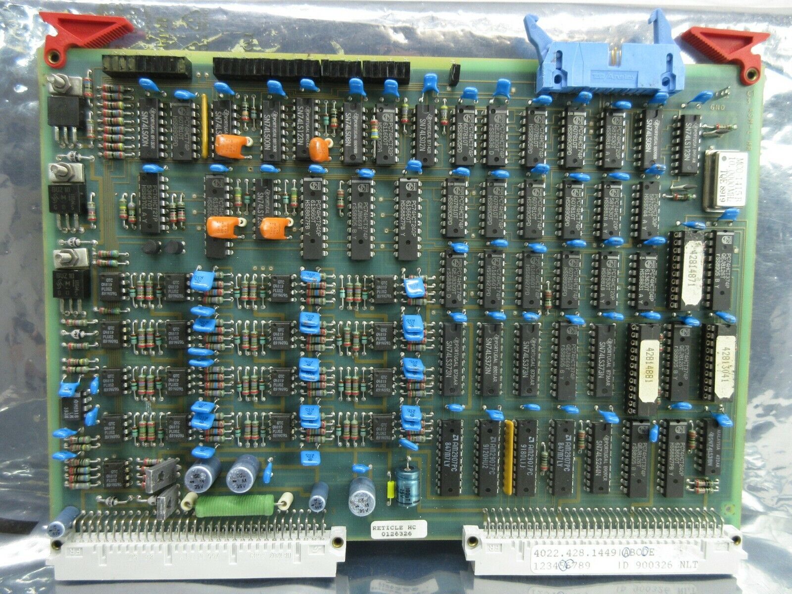
ASML 4022.428.1276是ASML专为先进制程半导体制造设计的高精度晶圆步进系统,核心特性包括:
亚微米级定位精度:重复定位精度≤0.05μm,支持28nm以下制程晶圆传输。
多规格兼容性:适配300mm及以下晶圆,厚度范围300~800μm,兼容硅、化合物半导体等基材。
高可靠性设计:无故障运行时间(MTBF)≥5000小时,耐受真空环境(<1e-5 mbar)。
产品详细说明
1.技术架构与核心功能
运动控制单元:
基于线性马达与磁悬浮技术,实现X/Y/Z三轴运动,定位速度≤200mm/s,加速度≤10g。
闭环反馈系统集成激光干涉仪(分辨率0.1nm)与压电陶瓷微调模块,动态跟踪误差≤0.1μm。
晶圆承载系统:
真空吸附盘设计,吸附力≥50mbar,支持晶圆边缘检测与自动对齐。
温控模块维持晶圆温度±0.5℃波动,减少热应力导致的形变。
环境适应性设计:
氦气循环冷却系统,有效降低运动部件温漂至≤0.01μm/K。
碳纤维复合材料框架,抗振性能≥100Hz。
2.性能突破
传输效率:
单晶圆处理时间≤3秒(含定位与对齐),产能提升至300片/小时(200mm晶圆)。
良率保障:
晶圆表面划伤率≤0.01%,边缘崩边控制≤5μm。
跨代适配性:
兼容ASML TWINSCAN系列光刻机(如XT:1950i至NXE:3600D),支持多光刻工艺集成。
技术规格:ASML 4022.428.1276
参数项规格描述
定位精度重复定位≤0.05μm,单次定位≤0.1μm
运动范围X/Y轴±250mm,Z轴±50mm
环境耐受性真空耐受<1e-5 mbar,温度范围15~30℃
接口类型PCIe Gen4×16(控制接口)+RS-422(设备通信)
功耗≤500W(运行模式)
Product brief description
ASML 4022.428.1276 is a high-precision wafer stepping system designed by ASML for advanced process semiconductor manufacturing.The core features include:
Submicron-level positioning accuracy:Repeated positioning accuracy≤0.05μm,supports process wafer transmission below 28nm.
Multi-spec Compatibility:Suitable for wafers of 300mm or below,with a thickness range of 300~800μm,compatible with substrates such as silicon,compound semiconductors and other substrates.
High reliability design:Fault-free running time(MTBF)≥5000 hours,with vacuum environment(<1e-5 mbar).
Product details
1.Technical architecture and core functions
Motion control unit:
Based on linear motor and magnetic levitation technology,the three-axis movement of X/Y/Z is realized,with a positioning speed of≤200mm/s and an acceleration of≤10g.
The closed-loop feedback system integrates a laser interferometer(resolution 0.1nm)and a piezoelectric ceramic fine-tuning module,with dynamic tracking error≤0.1μm.
Wafer bearing system:
Vacuum adsorption disk design,adsorption force≥50mbar,supports wafer edge detection and automatic alignment.
The temperature control module maintains the wafer temperature fluctuations of±0.5℃to reduce deformation caused by thermal stress.
Environmental adaptability design:
The helium circulation cooling system effectively reduces the temperature drift of moving parts to≤0.01μm/K.
Carbon fiber composite frame,vibration resistance≥100Hz.
2.Performance breakthrough
Transmission efficiency:
The single wafer processing time is≤3 seconds(including positioning and alignment),and the production capacity is increased to 300 pieces per hour(200mm wafer).
Yield guarantee:
The scratch rate of the wafer surface is≤0.01%,and the edge collapse control is≤5μm.
Cross-generation adaptability:
Compatible with ASML TWINSCAN series lithography machines(such as XT:1950i to NXE:3600D),supports multi-lithography process integration.
Technical specifications:ASML 4022.428.1276
Parameters Specification Description
Positioning accuracy Repeated positioning≤0.05μm,single positioning≤0.1μm
Range of motion:X/Y axis±250mm,Z axis±50mm
Environmental tolerance Vacuum tolerance<1e-5 mbar,temperature range 15-30℃
Interface type PCIe Gen4×16(control interface)+RS-422(device communication)
Power consumption≤500W(operating mode)