
描述
产品简要说明
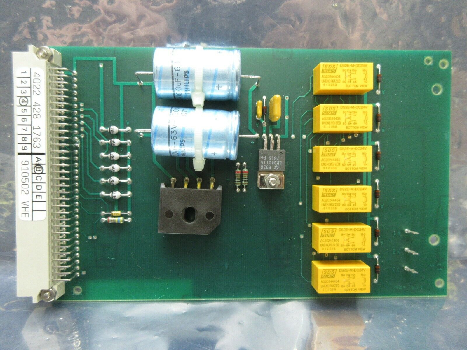
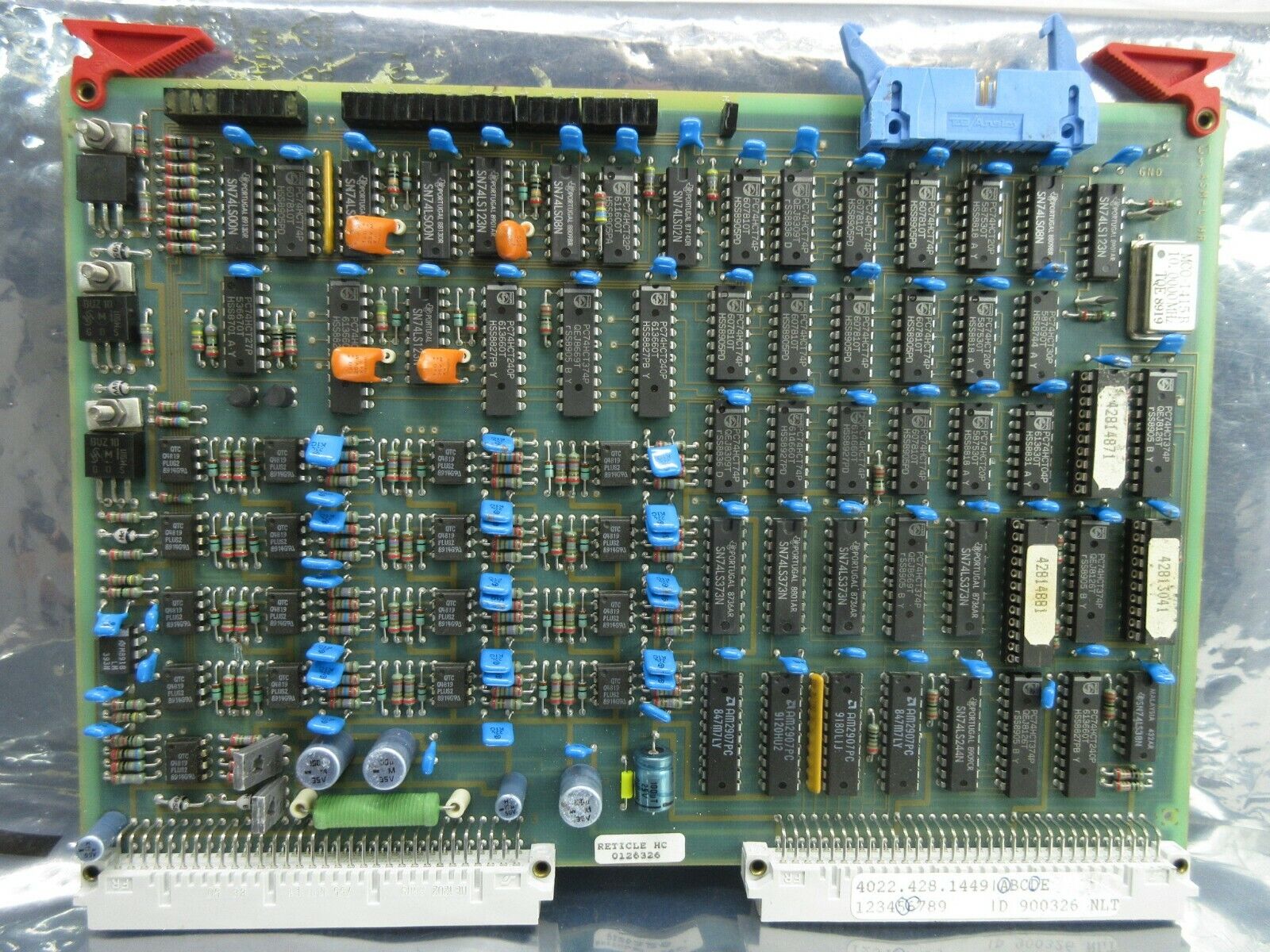
ASML 4022.428.1449是ASML为High NA EUV光刻机设计的光学透镜组,核心特性包括:
亚埃级光场聚焦:采用多层膜堆镀膜技术,能量透过率≥92%,波前畸变≤0.01λRMS。
极端环境耐受性:耐受真空环境(<1e-8 mbar)与高温辐射(局部耐受1200℃),材料应力变化≤0.002%。
自适应校正能力:集成实时波前传感与变形镜阵列,动态补偿误差≤0.05nm RMS。
产品详细说明
1.技术架构与核心功能
光学设计:
采用Zemax优化的12级透镜组,包含4组反射镜与8组透射镜,有效焦距1.2m,数值孔径(NA)0.55。
多层膜堆镀膜工艺(Mo/Si/Mo/Si),反射率≥68%(13.5nm波长)。
环境补偿系统:
磁悬浮支撑结构(振动隔离效率≥99.99%)与超低温冷却(液氦循环,温度波动≤±0.005℃)。
碳化硅基板与氮化铝涂层,抗热膨胀系数≤0.1ppm/℃。
智能控制单元:
基于FPGA的实时波前传感与变形镜驱动,响应时间<1ms。
自动校准算法,全参数标定时间≤8小时。
2.性能突破
光场质量:
多层叠加曝光(MLA)场景下,光斑均匀性≥95%(3σ),支持3nm制程图形转移。
能效优化:
热管理能耗降低40%,系统功耗≤200W(运行模式)。
跨代兼容性:
支持ASML NXE:4500(NA=0.55)至未来NA=0.75机型,预留光场扩展接口。
技术规格:ASML 4022.428.1449
参数项规格描述
工作波长13.5nm(EUV)
数值孔径(NA)0.55(可扩展至0.75)
能量透过率≥92%(13.5nm波长)
波前畸变≤0.01λRMS
环境耐受性真空耐受<1e-8 mbar,高温耐受1200℃(局部)
响应时间动态补偿响应<1ms
核心价值与性能亮点
1.High NA制程突破
多模态补偿机制:同步校正光场畸变、热漂移与振动干扰,支持3nm以下制程的纳米级图形转移。
AI驱动优化:通过强化学习模型预测光场动态变化,补偿响应速度提升至100μs。
2.全生命周期管理
模块化维护:变形镜与传感器可独立更换,维护时间≤4小时。
数字孪生支持:内置虚拟仿真模型,故障诊断准确率≥98%。
3.行业生态兼容
跨平台适配:兼容台积电、三星等主流晶圆厂的光刻工艺参数库。
工业互联网集成:支持OPC UA与TDM协议,实现与MES系统的实时数据交互。
Product brief description
ASML 4022.428.1449 is an optical lens group designed by ASML for High NA EUV lithography machines.The core features include:
Subangia-level light field focusing:multi-layer film stack coating technology is used,with energy transmittance≥92%,wavefront distortion≤0.01λRMS.
Extreme environmental tolerance:Tolerate vacuum environment(<1e-8 mbar)and high temperature radiation(local tolerance to 1200℃),material stress change≤0.002%.
Adaptive correction capability:Integrated real-time wavefront sensing and deforming mirror array,dynamic compensation error≤0.05nm RMS.
Product details
1.Technical architecture and core functions
Optical design:
A 12-level lens group optimized by Zemax is adopted,including 4 groups of reflectors and 8 groups of transmitters,with an effective focal length of 1.2m and a numerical aperture(NA)of 0.55.
Multi-layer film stack coating process(Mo/Si/Mo/Si),reflectivity≥68%(13.5nm wavelength).
Environmental Compensation System:
Magnetic levitation support structure(vibration isolation efficiency≥99.99%)and ultra-low temperature cooling(liquid helium circulation,temperature fluctuation≤±0.005℃).
Silicon carbide substrate and aluminum nitride coating,thermal expansion coefficient≤0.1ppm/℃.
Intelligent control unit:
Real-time wavefront sensing and deforming mirror drive based on FPGA,response time<1ms.
Automatic calibration algorithm,full parameter calibration time≤8 hours.
2.Performance breakthrough
Light field mass:
In multi-layer superimposed exposure(MLA)scenario,the spot uniformity is≥95%(3σ),supporting 3nm process graphic transfer.
Energy efficiency optimization:
Thermal management energy consumption is reduced by 40%,and the system power consumption is≤200W(operation mode).
Cross-generation compatibility:
Supports ASML NXE:4500(NA=0.55)to future NA=0.75 models,and reserves light field expansion interface.
Technical specifications:ASML 4022.428.1449
Parameters Specification Description
Operating wavelength:13.5nm(EUV)
Numerical aperture(NA)0.55(scalable to 0.75)
Energy transmittance≥92%(13.5nm wavelength)
Wavefront distortion≤0.01λRMS
Environmental tolerance Vacuum tolerance<1e-8 mbar,high temperature tolerance 1200℃(local)
Response time Dynamic compensation response<1ms
Core Valuesand Performance Highlights
1.High NA process breakthrough
Multimodal compensation mechanism:synchronously corrects light field distortion,thermal drift and vibration interference,and supports nanoscale pattern transfer in processes below 3nm.
AI-driven optimization:predict dynamic changes in the light field through reinforcement learning model,and the compensation response speed is increased to 100μs.
2.Full life cycle management
Modular maintenance:The deforming mirror and sensor can be replaced independently,and the maintenance time is≤4 hours.
Digital twin support:built-in virtual simulation model,fault diagnosis accuracy rate≥98%.
3.Industry ecology compatibility
Cross-platform adaptation:compatible with the lithography process parameter library of mainstream wafer factories such as TSMC and Samsung.
Industrial Internet integration:supports OPC UA and TDM protocols to realize real-time data interaction with the MES system.