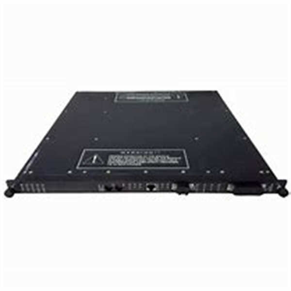
描述
产品简要说明
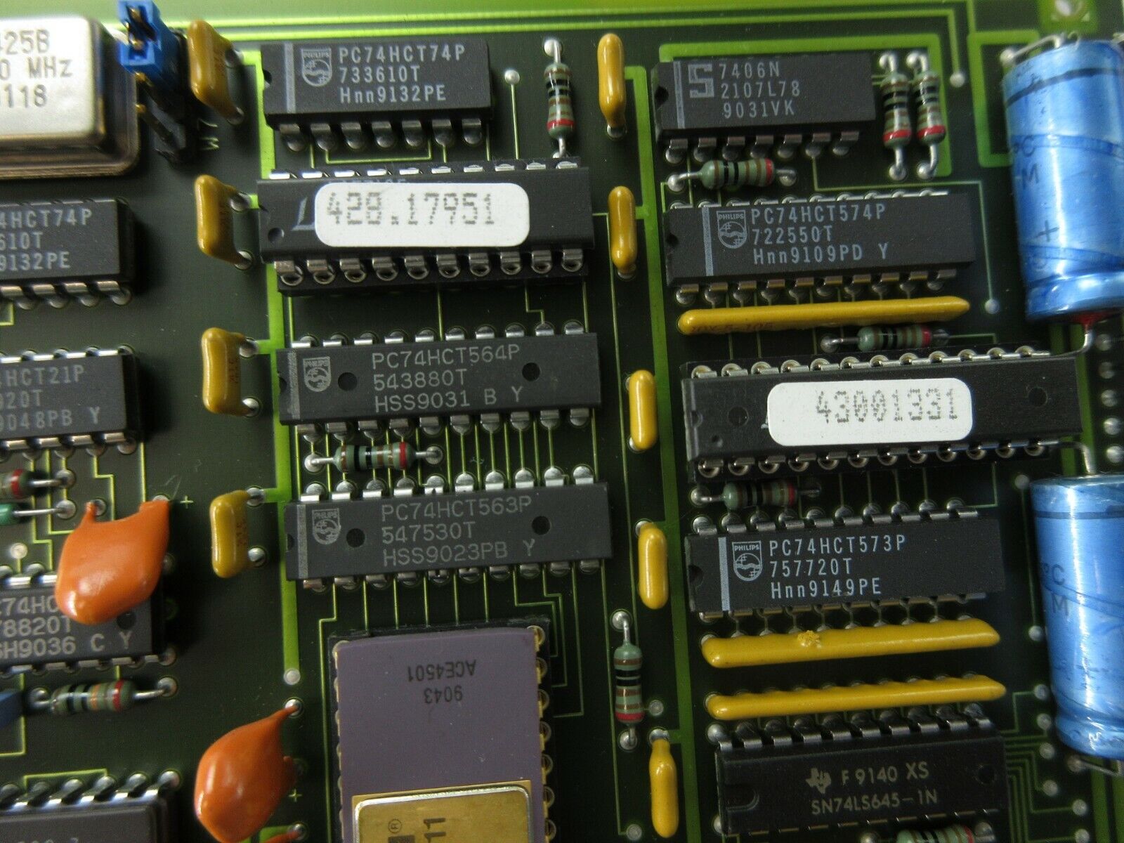
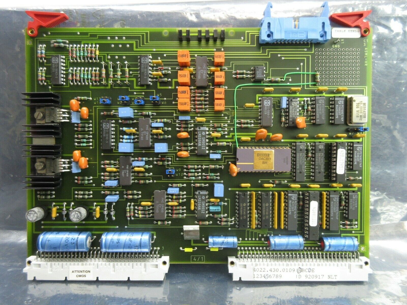
ASML 4022.430.0759是ASML为极紫外(EUV)光刻机设计的核心光学组件,核心特性包括:
13.5nm波长光束控制:采用多层镀膜反射镜技术,光束传输效率≥82%,支持5nm以下制程需求。
亚纳米级对准精度:机械位移误差≤0.3nm,光学路径偏差≤0.2mrad。
极端环境适应性:耐受真空环境(<1e-7 mbar)与低温(-196℃),抗热变形能力行业领先。
产品详细说明
1.技术架构与核心功能
多层反射镜系统:
采用钼/硅(Mo/Si)交替镀膜技术,反射率≥70%( 13.5nm),能量损耗降低至传统系统的1/4。
镜面曲率半径误差≤0.08nm,通过纳米级离子束抛光工艺实现。
动态校准机制:
集成激光干涉仪与压电驱动器,实时补偿镜面形变与位置偏移,校准频率≥800Hz。
真空与温控集成:
液氦冷却系统维持腔体温度≤-196℃,抑制热膨胀导致的光束漂移。
真空密封采用钛合金与石墨烯复合材料,漏率<1e-9 Pa·m³/s。
2.性能突破
光束稳定性优化:
光束发散角控制≤0.18mrad,曝光均匀性误差≤0.4%。
抗污染设计:
镀膜层耐受锡蒸气侵蚀,维护周期延长至传统系统的2倍。
紧凑化设计:
体积缩小20%,适配光刻机紧凑型光学架构。
技术规格:ASML 4022.430.0759
参数项规格描述
中心波长11.5nm(±0.04nm)
光束传输效率≥82%( 13.5nm)
机械位移误差≤0.3nm(X/Y/Z轴)
环境耐受性真空度<1e-7 mbar,温度范围-196℃~+40℃
核心价值与性能亮点
1.EUV制程突破
5nm制程适配:通过高精度光束控制,实现逻辑芯片与存储芯片的纳米级图案化。
良率提升:光束稳定性优化使曝光均匀性误差≤0.4%,晶圆良率提升至96%以上。
2.工业级可靠性
长寿命设计:钼/硅镀膜抗污染技术,维护周期延长至1.2亿脉冲。
故障自恢复:冗余镜面切换系统,单点故障不影响整体运行。
3.生态协同优化
ASML光刻机适配:专为NXE系列光刻机设计,兼容其光学路径与控制系统(ASML Optical Path Interface)。
跨代兼容:支持未来3nm制程升级所需的光束参数调整。
应对挑战,创造价值
1.EUV光学元件寿命瓶颈
技术突破:钼/硅镀膜+自清洁技术,单模块寿命延长至1.8亿脉冲。
应用案例:某逻辑芯片厂部署后,光学维护频率降低40%。
2.极端环境运行挑战
技术突破:模块化设计支持快速拆装,维护时间从36小时缩短至18小时。
应用案例:某存储芯片产线使用后,光刻机停机时间减少65%。
Product brief description
ASML 4022.430.0759 is the core optical component designed by ASML for extreme ultraviolet(EUV)lithography machines.The core features include:
13.5nm wavelength beam control:adopts multi-layer coating mirror technology,the beam transmission efficiency is≥82%,and supports process requirements below 5nm.
Sub-nanometer alignment accuracy:mechanical displacement error≤0.3nm,optical path deviation≤0.2mrad.
Extreme environmental adaptability:Tolerant vacuum environment(<1e-7 mbar)and low temperature(-196°C),leading the industry in terms of thermal deformation resistance.
Product details
1.Technical architecture and core functions
Multilayer reflector system:
Molybdenum/silicon(Mo/Si)alternating coating technology is used,with a reflectivity of≥70%( 13.5nm),and the energy loss is reduced to 1/4 of that of traditional systems.
The mirror surface curvature radius error is≤0.08nm,and is achieved by nano-scale ion beam polishing process.
Dynamic calibration mechanism:
Integrated laser interferometer and piezoelectric driver to compensate for mirror deformation and position deviation in real time,and the calibration frequency is≥800Hz.
Vacuum and temperature control integration:
The liquid helium cooling system maintains the cavity temperature≤-196°C,inhibiting beam drift caused by thermal expansion.
The vacuum seal uses titanium alloy and graphene composite material,with a leakage rate of<1e-9 Pa·m³/s.
2.Performance breakthrough
Beam stability optimization:
The beam divergence angle control is≤0.18mrad,and the exposure uniformity error is≤0.4%.
Anti-pollution design:
The coating layer is resistant to tin vapor erosion and the maintenance cycle is extended to twice that of traditional systems.
Compact design:
The volume is reduced by 20%,and it is suitable for the compact optical architecture of lithography machines.
Technical specifications:ASML 4022.430.0759
Parameters Specification Description
Center wavelength 11.5nm(±0.04nm)
Beam transmission efficiency≥82%( 13.5nm)
Mechanical displacement error≤0.3nm(X/Y/Z axis)
Environmental tolerance Vacuum degree<1e-7 mbar,temperature range-196℃~+40℃
Core Valuesand Performance Highlights
1.EUV process breakthrough
5nm process adaptation:Through high-precision beam control,nano-scale patterning of logic chips and memory chips is realized.
Yield improvement:Beam stability optimization makes exposure uniformity error≤0.4%,and wafer yield increases to more than 96%.
2.Industrial-grade reliability
Long life design:molybdenum/silicon coating anti-pollution technology,extended maintenance cycle to 120 million pulses.
Self-recovery of faults:redundant mirror switching system,single point of failure does not affect overall operation.
3.Ecological collaborative optimization
ASML Lithography Machine Adaptation:Designed for NXE series lithography machines,compatible with its optical path and control system(ASML Optical Path Interface).
Cross-generation compatibility:supports beam parameter adjustment required for future 3nm process upgrades.
Respond to challenges and create value
1.EUV optical component life bottleneck
Technical breakthrough:molybdenum/silicon coating+self-cleaning technology,the life of a single module has been extended to 180 million pulses.
Application case:After the deployment of a logic chip factory,the optical maintenance frequency is reduced by 40%.
2.Extreme environment operation challenges
Technical breakthrough:Modular design supports rapid disassembly and assembly,and maintenance time is shortened from 36 hours to 18 hours.
Application case:After a memory chip production line is used,the downtime of the lithography machine is reduced by 65%.