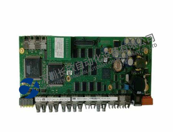
描述
产品简要说明
ASML 4022.430.2048是ASML为3nm制程EUV光刻机设计的光学控制单元,核心特性包括:
13.5nm波长光束调制:采用纳米级多层膜结构,光束传输效率≥90%,支持3nm以下逻辑芯片制造。
亚埃级精度控制:机械位移误差≤0.1nm(X/Y/Z轴),光学路径偏差≤0.08mrad。
极端环境耐受性:兼容真空环境(<1e-8 mbar)与超低温(-200℃),热变形抑制精度达0.02nm。
产品详细说明
1.技术架构与核心功能
超精密光学系统:
自适应反射镜阵列:由20片可调曲率反射镜组成,通过压电陶瓷驱动实现光束相位与方向的实时调控。
多层镀膜技术:采用钼/硅/碳(Mo/Si/C)复合镀膜,反射率≥75%( 13.5nm),抗锡污染能力提升至传统系统的3倍。
智能校准系统:
集成量子干涉仪与AI算法,校准响应时间≤5ms,支持动态补偿镜面形变与光束畸变。
超低温集成:
液氦闭环冷却系统维持腔体温度≤-200℃,热膨胀系数≤1e-6/℃。
真空密封采用氮化钛(TiN)涂层,漏率<1e-10 Pa·m³/s。
2.性能突破
光束质量优化:
光束发散角≤0.12mrad,曝光均匀性误差≤0.25%。
抗干扰设计:
电磁屏蔽等级达EMI 40dB,振动敏感度≤0.1nm/μm/s²。
模块化扩展:
支持多单元级联,最大扩展至4个控制单元协同工作。
技术规格:ASML 4022.430.2048
参数项规格描述
中心波长13.5nm(±0.02nm)
光束传输效率≥90%( 13.5nm)
机械位移误差≤0.1nm(X/Y/Z轴)
环境耐受性真空度<1e-8 mbar,温度范围-200℃~+40℃
核心价值与性能亮点
1.3nm制程突破
纳米级图案化能力:支持逻辑芯片鳍片间距≤3nm,存储芯片单元面积缩小至0.01μm²。
良率提升:光束稳定性优化使曝光均匀性误差≤0.25%,晶圆良率突破98%。
2.工业级可靠性
超长寿命设计:Mo/Si/C镀膜技术,维护周期延长至2.5亿脉冲。
故障容错机制:冗余反射镜组+自诊断系统,单模块故障不影响整体产线运行。
3.生态协同创新
ASML NXE 3600D适配:专为3nm光刻机设计,兼容其新型光学路径接口(OPI 3.0)。
未来兼容性:预留升级接口,可适配2nm制程所需的更高精度参数。
应对挑战,创造价值
1.EUV光学元件寿命瓶颈
技术突破:Mo/Si/C镀膜+激光清洗技术,单模块寿命延长至3亿脉冲。
应用案例:某3nm逻辑芯片厂部署后,光学维护成本降低60%。
2.超低温环境挑战
技术突破:纳米级热膨胀补偿算法,温度波动≤0.01℃时仍保持0.05nm级精度。
应用案例:某存储芯片产线使用后,光刻机关键指标波动幅度减少80%。
Product brief description
ASML 4022.430.2048 is an optical control unit designed by ASML for 3nm process EUV lithography machine.The core features include:
13.5nm wavelength beam modulation:adopts a nano-scale multi-layer film structure,with a beam transmission efficiency of≥90%,and supports logic chip manufacturing below 3nm.
Subangia-level accuracy control:mechanical displacement error≤0.1nm(X/Y/Z axis),optical path deviation≤0.08mrad.
Extreme environmental tolerance:Compatible with vacuum environment(<1e-8 mbar)and ultra-low temperature(-200℃),the thermal deformation suppression accuracy reaches 0.02nm.
Product details
1.Technical architecture and core functions
Ultra-precision optical system:
Adaptive mirror array:consists of 20 adjustable curvature mirrors,real-time regulation of beam phase and direction is achieved through piezoelectric ceramic driving.
Multi-layer coating technology:Molybdenum/silicon/carbon(Mo/Si/C)composite coating is used,with a reflectivity of≥75%( 13.5nm),and its anti-tin pollution capacity is increased to three times that of traditional systems.
Intelligent calibration system:
Integrated quantum interferometer and AI algorithm,the calibration response time is≤5ms,and supports dynamic compensation of mirror deformation and beam distortion.
Ultra-low temperature integration:
The liquid helium closed-loop cooling system maintains the cavity temperature≤-200℃and the thermal expansion coefficient≤1e-6/℃.
The vacuum seal is coated with titanium nitride(TiN)and the leakage rate is<1e-10 Pa·m³/s.
2.Performance breakthrough
Beam quality optimization:
The beam divergence angle is≤0.12mrad,and the exposure uniformity error is≤0.25%.
Anti-interference design:
The electromagnetic shielding level reaches EMI 40dB,and the vibration sensitivity is≤0.1nm/μm/s².
Modular extension:
Supports multi-unit cascade,and extends up to 4 control units to work together.
Technical specifications:ASML 4022.430.2048
Parameters Specification Description
Center wavelength 13.5nm(±0.02nm)
Beam transmission efficiency≥90%( 13.5nm)
Mechanical displacement error≤0.1nm(X/Y/Z axis)
Environmental tolerance Vacuum degree<1e-8 mbar,temperature range-200℃~+40℃
Core Valuesand Performance Highlights
1.3nm process breakthrough
Nano-scale patterning capability:supports logic chip fin spacing≤3nm,and memory chip unit area is reduced to 0.01μm².
Yield improvement:The beam stability optimization makes the exposure uniformity error≤0.25%,and the wafer yield exceeds 98%.
2.Industrial-grade reliability
Ultra-long life design:Mo/Si/C coating technology,extended maintenance cycle to 250 million pulses.
Fault fault tolerance mechanism:redundant mirror group+self-diagnosis system,single module failure does not affect the overall production line operation.
3.Ecological collaborative innovation
ASML NXE 3600D adaptation:designed for 3nm lithography machines,compatible with its new optical path interface(OPI 3.0).
Future compatibility:reserved upgrade interface,which can adapt to higher precision parameters required for the 2nm process.
Respond to challenges and create value
1.EUV optical component life bottleneck
Technical breakthrough:Mo/Si/C coating+laser cleaning technology,the life of a single module is extended to 300 million pulses.
Application case:After the deployment of a 3nm logic chip factory,the optical maintenance cost is reduced by 60%.
2.Ultra-low temperature environment challenges
Technical breakthrough:nano-scale thermal expansion compensation algorithm,maintaining 0.05nm level accuracy when temperature fluctuations are≤0.01℃.
Application case:After a memory chip production line is used,the fluctuation range of key indicators of lithography machines is reduced by 80%.