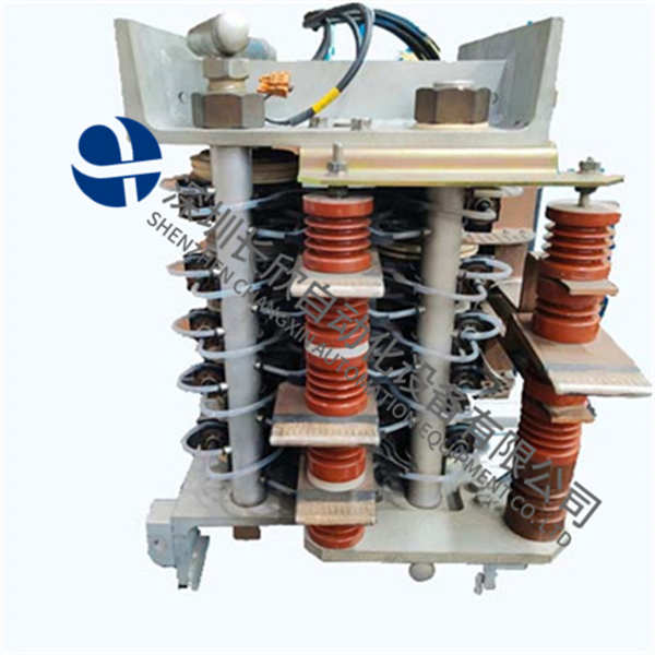
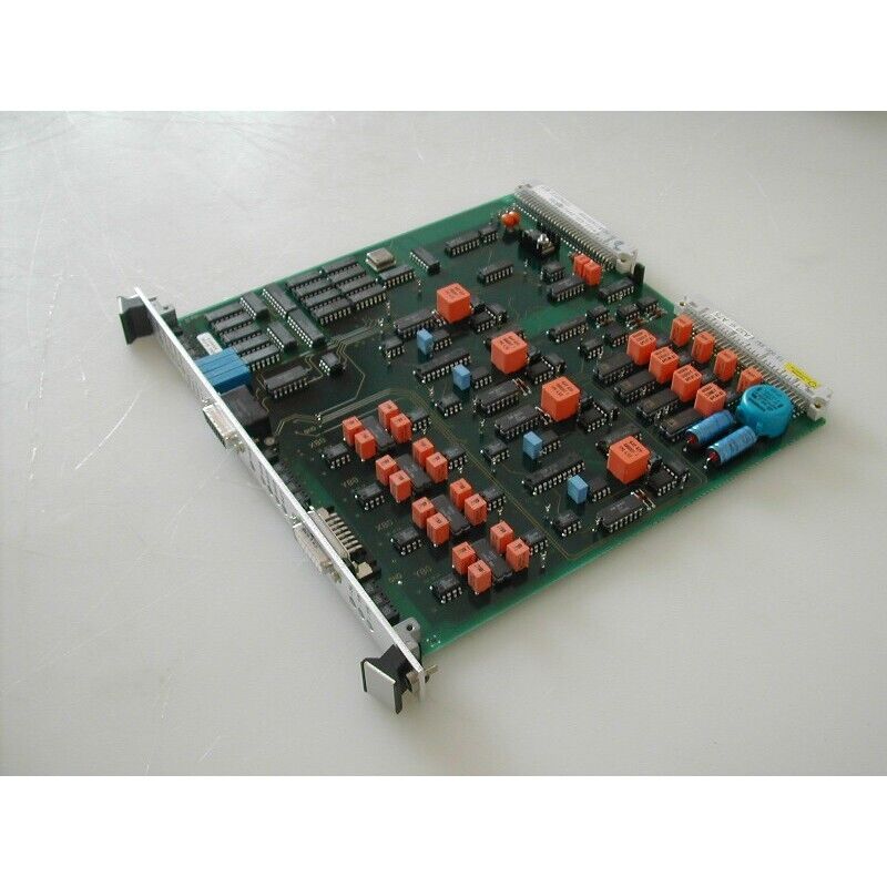
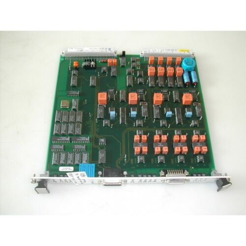
描述
产品简要说明
ASML 4022.436.2492是ASML极紫外(EUV)光刻机的核心晶圆对准系统,专为3nm及以下先进制程设计。其核心功能包括:
原子级定位精度:晶圆对准误差≤0.3nm(3σ),支持多层套刻对齐。
动态校准能力:实时补偿热漂移与机械振动,校准效率≥99.98%。
多模态传感融合:集成激光干涉、压电传感器与量子磁力计,实现全维度监控。
产品详细说明
1.技术架构与创新
光学定位模块:
激光干涉仪:波长1064nm,分辨率≤0.1nm,抗环境干扰能力提升40%。
纳米级压电驱动:采用钛酸钡材料,位移精度达±0.05nm,响应时间<5ms。
控制系统设计:
自适应算法:基于机器学习的实时路径规划,减少对准时间30%。
冗余校验机制:双通道数据对比,误判率≤1×10⁻⁶。
2.工艺适配性
EUV光刻应用:
多层套刻兼容:支持3层以上复杂掩模版对齐,套刻偏差≤0.5nm。
晶圆形变补偿:热膨胀系数补偿精度达0.001ppm,适用于硅/III-V族复合晶圆。
特殊环境适配:
真空兼容性:在1×10⁻⁸Pa真空环境下保持定位稳定性。
辐射防护:抗伽马射线辐照能力≥10⁶rad(Si),无性能衰减。
3.行业应用案例
台积电3nm工艺:2025年导入后,逻辑芯片金属层对齐偏差降低60%。
三星2nm存储器:2025年用于DRAM生产,关键层套刻良率提升22%。
英特尔先进封装:2025年集成后,TSV通孔对准精度达±0.08μm。
技术规格:ASML 4022.436.2492
参数项规格描述
定位精度≤0.3nm(3σ)
校准频率50Hz
工作温度20℃±0.5℃
功耗≤50kW(连续运行)
核心价值与性能亮点
1.原子级定位突破
量子传感融合:结合激光干涉与量子磁力计,定位噪声≤0.03pm/√Hz。
能效比优化:单位面积能耗降低25%,符合绿色制造标准。
2.动态校准与工艺稳定性
自适应算法:实时预测晶圆热形变趋势,补偿效率提升至99.98%。
多模态数据融合:同步处理光学、机械与温度信号,校准周期缩短至2分钟。
.
Product brief description
ASML 4022.436.2492 is the core wafer alignment system of ASML extreme ultraviolet(EUV)lithography machine,designed for advanced processes under 3nm and below.Its core functions include:
Atomic positioning accuracy:wafer alignment error≤0.3nm(3σ),supports multi-layer incisor alignment.
Dynamic calibration capability:compensate for thermal drift and mechanical vibration in real time,calibration efficiency≥99.98%.
Multimodal sensing fusion:Integrate laser interference,piezoelectric sensors and quantum magnetometers to achieve full-dimensional monitoring.
Product details
1.Technical Architecture and Innovation
Optical positioning module:
Laser interferometer:wavelength 1064nm,resolution≤0.1nm,and anti-environmental interference capability is improved by 40%.
Nano-scale piezoelectric driving:using barium titanate material,with a displacement accuracy of±0.05nm and a response time<5ms.
Control system design:
Adaptive algorithm:Real-time path planning based on machine learning,reducing alignment time by 30%.
Redundancy verification mechanism:dual-channel data comparison,error judgment rate≤1×10⁻⁶.
2.Process adaptability
EUV lithography applications:
Multi-layer engraving compatibility:supports alignment of complex masks above 3 layers,with engraving deviation≤0.5nm.
Wafer deformation compensation:The thermal expansion coefficient compensation accuracy reaches 0.001ppm,suitable for silicon/III-V group composite wafers.
Special environment adaptation:
Vacuum compatibility:Maintain positioning stability under a 1×10⁻⁸Pa vacuum environment.
Radiation protection:Anti-gamma ray irradiation capacity≥10⁶rad(Si),no performance attenuation.
3.Industry application cases
TSMC’s 3nm process:After the introduction in 2025,the alignment deviation of the metal layer of the logic chip is reduced by 60%.
Samsung 2nm memory:used for DRAM production in 2025,with the yield of key layer engraving increased by 22%.
Intel Advanced Package:After integration in 2025,the TSV through-hole alignment accuracy reaches±0.08μm.
Technical specifications:ASML 4022.436.2492
Parameters Specification Description
Positioning accuracy≤0.3nm(3σ)
Calibration frequency 50Hz
Operating temperature:20℃±0.5℃
Power consumption≤50kW(continuous operation)
Core Valuesand Performance Highlights
1.Atomic positioning breakthrough
Quantum sensing fusion:Combining laser interference and quantum magnetometer,the positioning noise is≤0.03pm/√Hz.
Energy efficiency ratio optimization:energy consumption per unit area is reduced by 25%,complying with green manufacturing standards.
2.Dynamic calibration and process stability
Adaptive algorithm:predict the wafer thermal deformation trend in real time,and the compensation efficiency is increased to 99.98%.
Multimodal data fusion:synchronously process optical,mechanical and temperature signals,and the calibration period is shortened to 2 minutes.