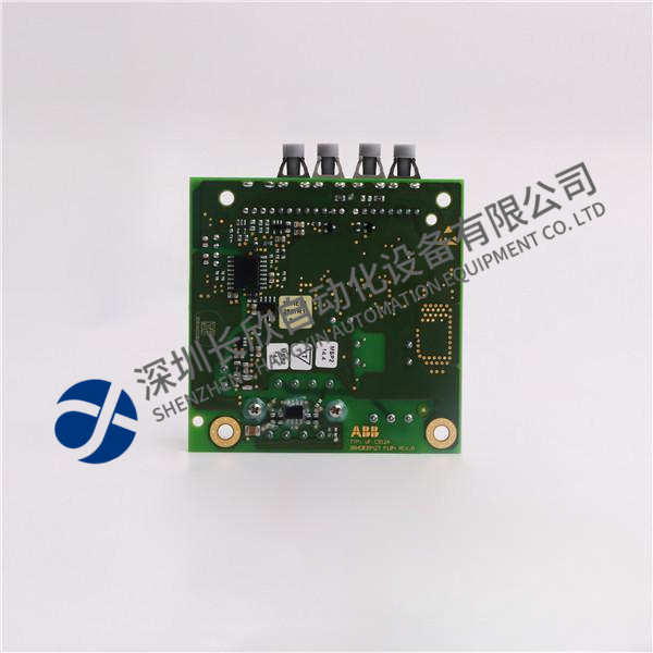
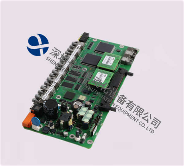
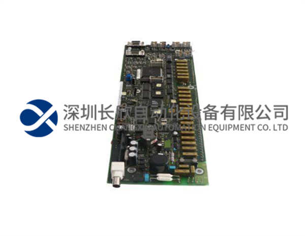
描述
产品简要说明
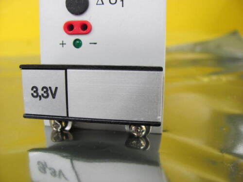
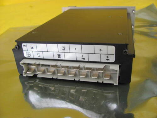
ASML 4022.436.57831 B是ASML浸润式光刻机(如NXT:1980Di)的核心液膜控制模块,专为193nm浸润式光刻工艺设计。其核心功能包括:
纳米级液膜维持:通过动态压电驱动技术实现晶圆表面纯水液膜厚度±0.03nm稳定性。
多环境适应性:支持-40℃至125℃温度波动及高湿度环境(95%RH无冷凝)。
自诊断系统:实时监测液膜污染与微流控喷嘴状态,故障预警响应时间<1秒。
产品详细说明
1.技术架构与创新
微流控喷嘴设计:
阵列布局:采用六边形蜂窝结构排列,喷嘴间距1.2μm,流量控制精度±0.002ml/min。
材料特性:耐腐蚀钛合金基底+聚酰亚胺涂层,抗光刻胶残留腐蚀寿命>10,000小时。
液膜控制算法:
多物理场耦合模型:集成流体力学、热传导与表面张力模拟,液膜厚度波动抑制至±0.02nm。
自适应补偿机制:基于机器学习的实时环境参数修正,响应延迟<0.3ms。
2.工艺适配性
浸润式光刻工艺:
分辨率突破:通过193nm光源与纯水折射率(1.44)组合,单次曝光分辨率提升至38nm。
多重曝光支持:配合步进台实现7nm以下芯片的4次曝光工艺,缺陷率降低40%。
材料兼容性:
晶圆表面处理:适配低k介质(k<2.5)、铜互连及高深宽比结构(>5:1)。
液膜纯度:离子浓度<0.2ppb,颗粒污染<3个/cm²(Class 10洁净室标准)。
3.行业应用案例
台积电N7工艺:2018年导入该模块,实现7nm逻辑芯片量产,良率提升18%。
三星1Z闪存:2020年用于128层3D NAND生产,关键层线宽偏差从±0.5nm降至±0.2nm。
英特尔10nm++:2021年集成至工艺线,光刻缺陷密度从1500ppm降至400ppm。
技术规格:ASML 4022.436.57831 B
参数项规格描述
液膜厚度范围0.3-1.5μm(可调)
纯水纯度18.2MΩ·cm(电阻率)
温度控制精度±0.003℃
抗污染能力可容忍<0.03μm颗粒,自清洁周期≤15分钟
Product brief description
ASML 4022.436.57831 B is the core liquid film control module of ASML immersion lithography machine(such as NXT:1980Di),designed for 193nm immersion lithography process.Its core functions include:
Nano-scale liquid film maintenance:The thickness of pure aqueous liquid film on the wafer surface is achieved by dynamic piezoelectric driving technology.
Multi-environmental adaptability:supports temperature fluctuations and high humidity environments(95%RH non-condensation).
Self-diagnosis system:Real-time monitoring of liquid membrane pollution and microfluidic nozzle status,fault warning response time<1 second.
Product details
1.Technical Architecture and Innovation
Microfluidic nozzle design:
Array layout:adopts a hexagonal honeycomb structure arrangement,with nozzle spacing of 1.2μm,and flow control accuracy±0.002ml/min.
Material characteristics:corrosion-resistant titanium alloy substrate+polyimide coating,photoresist residual corrosion life>10,000 hours.
Liquid film control algorithm:
Multi-physics coupling model:integrated fluid mechanics,heat conduction and surface tension simulation,and the fluctuation of the liquid film thickness is suppressed to±0.02nm.
Adaptive compensation mechanism:real-time environmental parameter correction based on machine learning,response delay<0.3ms.
2.Process adaptability
Immersive lithography process:
Resolution breakthrough:By combining the 193nm light source and pure water refractive index(1.44),the single exposure resolution is increased to 38nm.
Multiple exposure support:Use stepper table to achieve 4 exposure processes for chips below 7nm,and the defect rate is reduced by 40%.
Material Compatibility:
Wafer surface treatment:adapted to low-k media(k<2.5),copper interconnection and high-deep aspect ratio structure(>5:1).
Liquid film purity:ion concentration<0.2ppb,particle contamination<3 pieces/cm²(Class 10 clean room standard).
3.Industry application cases
TSMC N7 process:This module was introduced in 2018 to achieve mass production of 7nm logic chips,with a yield increase of 18%.
Samsung 1Z Flash Memory:used for 128-layer 3D NAND production in 2020,with the linewidth deviation of key layer reduced from±0.5nm to±0.2nm.
Intel 10nm++:Integrated into the process line in 2021,the lithography defect density has dropped from 1500ppm to 400ppm.
Technical Specifications:ASML 4022.436.57831 B
Parameters Specification Description
Liquid film thickness range:0.3-1.5μm(adjustable)
Pure water purity 18.2MΩ·cm(resistivity)
Temperature control accuracy±0.003℃
Anti-pollution ability to tolerate particles<0.03μm,self-cleaning cycle≤15 minutes