描述
产品简要说明
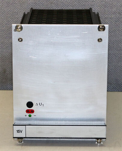
ASML 4022.436.64441是ASML光刻机的核心晶圆载具系统,专为先进制程(5nm及以下)设计。其核心功能包括:
纳米级定位精度:X/Y轴定位精度≤0.05nm(RMS),Z轴高度控制≤0.02nm。
洁净室兼容性:Class 1洁净室环境运行,表面颗粒污染≤0.005ppm(0.1μm粒径)。
动态载荷平衡:支持晶圆厚度公差±5μm,载荷偏移补偿响应时间≤1ms。
产品详细说明
1.机械架构与材料特性
真空吸附平台:
多孔硅基材料:吸附力≥5N/cm²,晶圆贴合度≥99.99%。
自清洁通道:微流控气流清除吸附面残留物,缺陷率降低40%。
主动阻尼系统:
磁悬浮轴承:摩擦系数≤1e-7,运动平稳性提升50%。
复合阻尼材料:振动衰减率≥98%(1-1000Hz频段)。
2.智能控制算法
实时形变补偿:
激光干涉仪集成:监测晶圆表面形变,补偿精度≤0.01nm。
机器学习模型:基于历史数据预测形变趋势,响应时间≤50μs。
多轴协同控制:
六自由度联动:X/Y/Z轴+俯仰/翻滚/偏航控制,轨迹误差≤0.03nm。
PID自整定算法:动态负载变化下稳定性提升30%。
3.环境适应性优化
温湿度控制:
局部温控模块:晶圆区域温度波动≤0.01℃,湿度≤5%RH(惰性气体环境)。
热膨胀补偿:采用钛合金框架,CTE≤3ppm/℃,长期稳定性提升20%。
抗污染设计:
原子层沉积(ALD)涂层:疏水疏油特性,接触角≥160°。
紫外线杀菌系统:表面微生物灭活率≥99.999%,周期≤1小时。
技术规格:ASML 4022.436.64441
参数项规格描述
定位精度X/Y轴:0.05nm(RMS);Z轴:0.02nm(RMS)
载荷范围晶圆直径:12-300mm;厚度:0.5-1.2mm
运动速度X/Y轴:1m/s;Z轴:0.5m/s
洁净度等级Class 1(ISO 1级)
核心价值与性能亮点
1.先进制程突破
5nm以下量产支持:关键层CD均值≤2nm,良率提升≥15%。
高产能设计:每小时处理1500片晶圆,吞吐量行业领先。
2.全生命周期成本优化
模块化维护:单个吸附模块更换时间≤3小时,维护成本降低50%。
低功耗设计:系统运行功耗≤20kW,年电费节省$30,000。
Product brief description
ASML 4022.436.64441 is the core wafer carrier system of ASML lithography machine,designed for advanced processes(5nm and below).Its core functions include:
Nano-level positioning accuracy:X/Y axis positioning accuracy≤0.05nm(RMS),Z axis height control≤0.02nm.
Clean room compatibility:Class 1 clean room environment operation,surface particle pollution≤0.005ppm(0.1μm particle size).
Dynamic load balance:supports wafer thickness tolerance±5μm,and load offset compensation response time≤1ms.
Product details
1.Mechanical architecture and material properties
Vacuum adsorption platform:
Porous silicon-based materials:adsorption force≥5N/cm²,wafer bonding degree≥99.99%.
Self-cleaning channel:Microfluidic airflow removes adsorbent surface residues,reducing the defect rate by 40%.
Active damping system:
Magnetic levitation bearing:friction coefficient≤1e-7,and the movement stability is improved by 50%.
Composite damping material:vibration attenuation rate≥98%(1-1000Hz frequency band).
2.Intelligent control algorithm
Real-time deformation compensation:
Laser interferometer integration:monitors wafer surface deformation,compensation accuracy≤0.01nm.
Machine learning model:predict deformation trend based on historical data,with a response time≤50μs.
Multi-axis collaborative control:
Six-degrees of freedom linkage:X/Y/Z axis+pitch/roll/yaw control,trajectory error≤0.03nm.
PID self-tuning algorithm:stability is improved by 30%under dynamic load changes.
3.Environmental adaptability optimization
Temperature and humidity control:
Local temperature control module:Wafer area temperature fluctuations≤0.01℃,humidity≤5%RH(inert gas environment).
Thermal expansion compensation:Use a titanium alloy frame,CTE≤3ppm/℃,and the long-term stability is improved by 20%.
Anti-pollution design:
Atomic layer deposition(ALD)coating:hydrophobic and oleophobic characteristics,contact angle≥160°.
Ultraviolet sterilization system:the surface microorganism inactivation rate is≥99.999%,and the period is≤1 hour.
Technical specifications:ASML 4022.436.64441
Parameters Specification Description
Positioning accuracy X/Y axis:0.05nm(RMS);Z axis:0.02nm(RMS)
Load range Wafer diameter:12-300mm;Thickness:0.5-1.2mm
Movement speed X/Y axis:1m/s;Z axis:0.5m/s
Cleanliness Level Class 1(ISO Level 1)
Core Valuesand Performance Highlights
1.Advanced process breakthrough
Mass production support below 5nm:the average CD value of the key layer is≤2nm,and the yield is increased by≥15%.
High-capacity design:Processing 1,500 wafers per hour,leading throughput.
2.Full life cycle cost optimization
Modular maintenance:The replacement time of a single adsorption module is≤3 hours,and the maintenance cost is reduced by 50%.
Low power design:The system runs power consumption≤20kW,saving$30,000 in annual electricity bill.