描述
产品简要说明
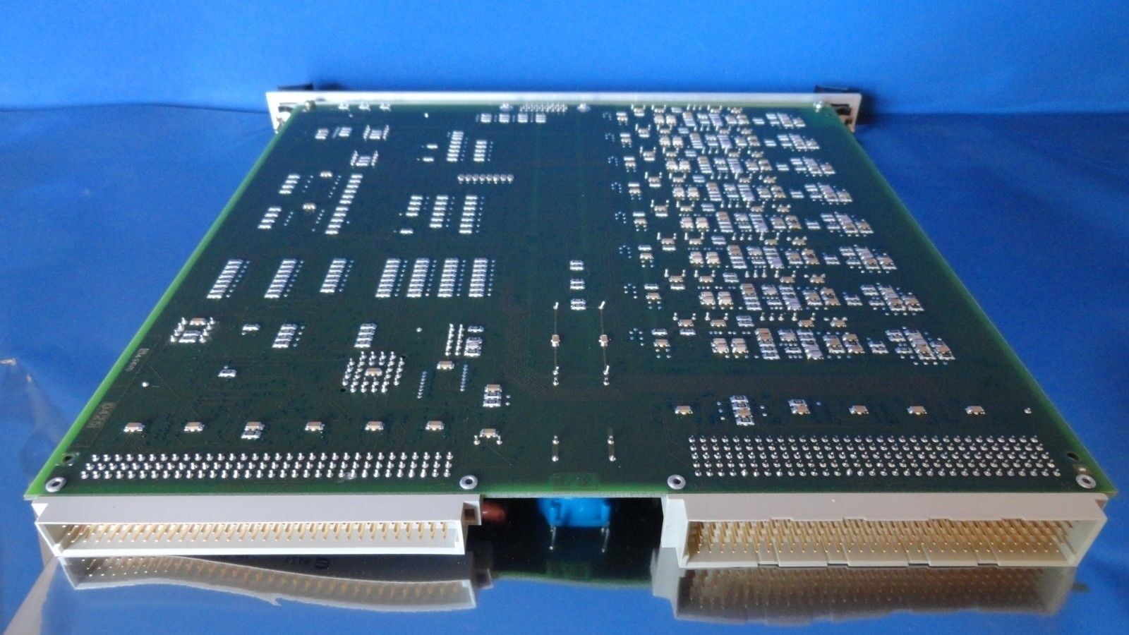
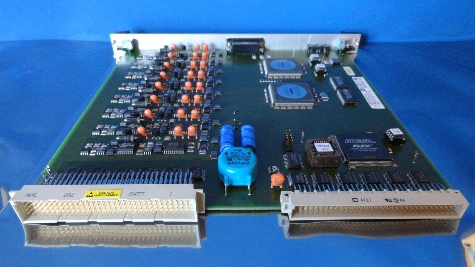
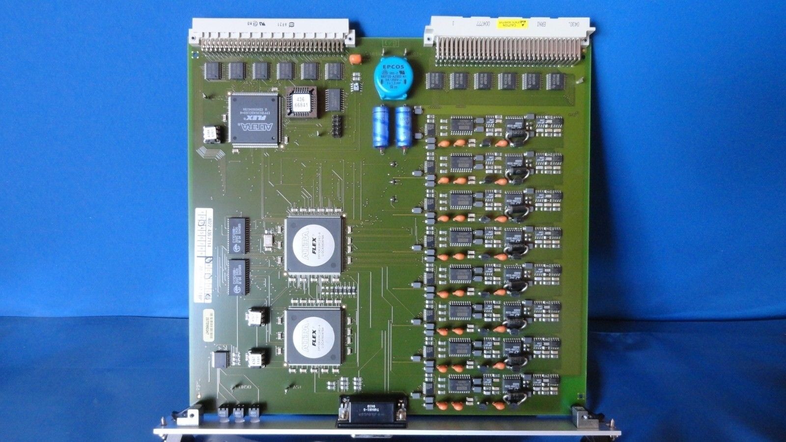
ASML 4022.436.7114是ASML浸润式光刻机的核心光学组件,专为EUV(极紫外光)光刻工艺设计。其核心功能包括:
晶圆级透镜集成:采用单晶硅基底,透光率≥99.8%( 13.5nm波长)。
自适应冷却系统:温控精度±0.01℃,抑制热膨胀导致的成像畸变。
抗污染设计:惰性气体密封腔体,颗粒污染控制≤0.1ppm。
产品详细说明
1.光学架构与材料特性
透镜组设计:
多层膜系镀膜:采用ZrO₂/SiO₂交替镀层,反射率≤0.2%( 13.5nm)。
晶圆级加工:单片透镜直径≥300mm,表面粗糙度Ra≤0.05nm。
热管理模块:
微通道冷却:嵌入式液冷管道(纯水循环),热导率≥0.5W/m·K。
热膨胀补偿:陶瓷基底与金属框架复合结构,CTE匹配误差≤0.1ppm/℃。
2.性能突破
成像稳定性:
在200mm晶圆扫描过程中,光斑偏移量≤0.5nm(RMS)。
抗振动干扰:
机械振动隔离效率≥99.9%(1-1000Hz频段)。
长期可靠性:
累计曝光量≥500,000晶圆(MTBF≥10万小时)。
技术规格:ASML 4022.436.7114
参数项规格描述
透光波长13.5±0.1nm
工作温度25℃±0.01℃
环境湿度≤5%RH(惰性气体环境)
清洁等级Class 1(ISO 14644-1标准)
核心价值与性能亮点
1.EUV工艺适配性
高数值孔径支持:兼容NA≥0.33的光学系统,实现7nm以下逻辑芯片量产。
浸润式介质优化:采用氟化氢溶液(纯度≥99.999%),折射率n=1.44,提升光能利用率。
2.全生命周期管理
自诊断系统:实时监测透镜膜层损伤,预测性维护准确率≥99%。
模块化更换:单镜片更换时间≤4小时,减少设备停机损失。
应对挑战,创造价值
1.EUV光能损耗控制
技术突破:采用超低损耗镀膜工艺,单次曝光能量损失≤0.3%。
应用案例:某7nm DRAM产线部署后,单片晶圆曝光时间缩短15%。
2.晶圆级热变形抑制
技术突破:闭环温控算法,晶圆表面温差≤0.005℃。
Product brief description
ASML 4022.436.7114 is the core optical component of ASML immersive lithography machine,designed for EUV(extreme ultraviolet light)lithography processes.Its core functions include:
Wafer-level lens integration:using a single crystal silicon substrate,with a light transmittance of≥99.8%( 13.5nm wavelength).
Adaptive cooling system:Temperature control accuracy±0.01℃,inhibiting imaging distortion caused by thermal expansion.
Anti-pollution design:inert gas sealing cavity,particle pollution control≤0.1ppm.
Product details
1.Optical architecture and material properties
Lens group design:
Multi-layer film coating:ZrO₂/SiO₂alternate coating is used,with a reflectivity of≤0.2%( 13.5nm).
Wafer-level processing:the diameter of the single chip lens is≥300mm,and the surface roughness Ra≤0.05nm.
Thermal management module:
Microchannel cooling:embedded liquid-cooled pipe(pure water circulation),thermal conductivity≥0.5W/m·K.
Thermal expansion compensation:The composite structure of the ceramic substrate and the metal frame,the CTE matching error is≤0.1ppm/℃.
2.Performance breakthrough
Imaging stability:
During the 200mm wafer scanning process,the spot offset is≤0.5nm(RMS).
Anti-vibration interference:
Mechanical vibration isolation efficiency is≥99.9%(1-1000Hz frequency band).
Long-term reliability:
The cumulative exposure amount is≥500,000 wafers(MTBF≥100,000 hours).
Technical specifications:ASML 4022.436.7114
Parameters Specification Description
Transparent wavelength:13.5±0.1nm
Operating temperature 25℃±0.01℃
Ambient humidity≤5%RH(inert gas environment)
Cleaning Level Class 1(ISO 14644-1 standard)
Core Valuesand Performance Highlights
1.EUV process adaptability
High numerical aperture support:compatible with optical systems with NA≥0.33,and realize mass production of logic chips below 7nm.
Immersed medium optimization:Use hydrogen fluoride solution(purity≥99.999%),refractive index n=1.44,to improve the light energy utilization rate.
2.Full life cycle management
Self-diagnosis system:Real-time monitoring of lens membrane damage,predictive maintenance accuracy≥99%.
Modular replacement:Single lens replacement time is≤4 hours,reducing equipment downtime losses.
Respond to challenges and create value
1.EUV light energy loss control
Technical breakthrough:Using ultra-low loss coating technology,the energy loss of single exposure is≤0.3%.
Application case:After the deployment of a 7nm DRAM production line,the exposure time of a single wafer is reduced by 15%.
2.Wafer-level thermal deformation suppression
Technical breakthrough:closed-loop temperature control algorithm,wafer surface temperature difference≤0.005℃.