描述
产品简要说明
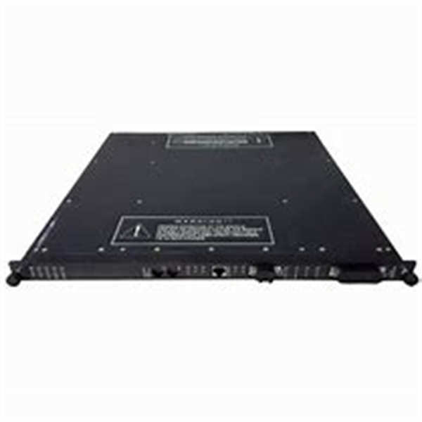
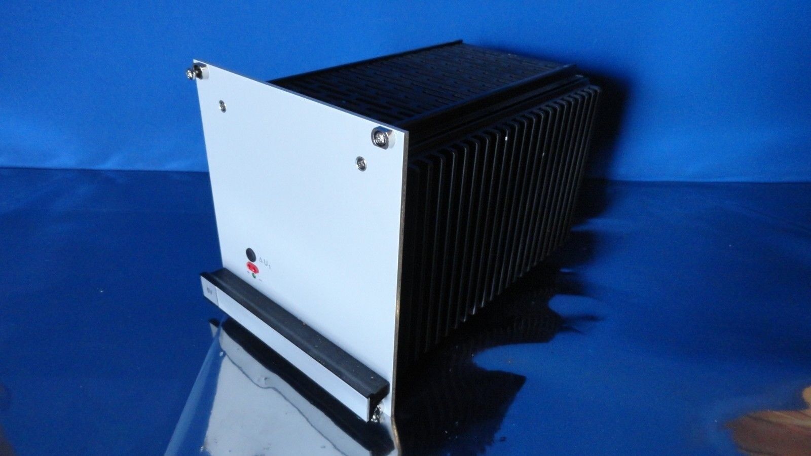
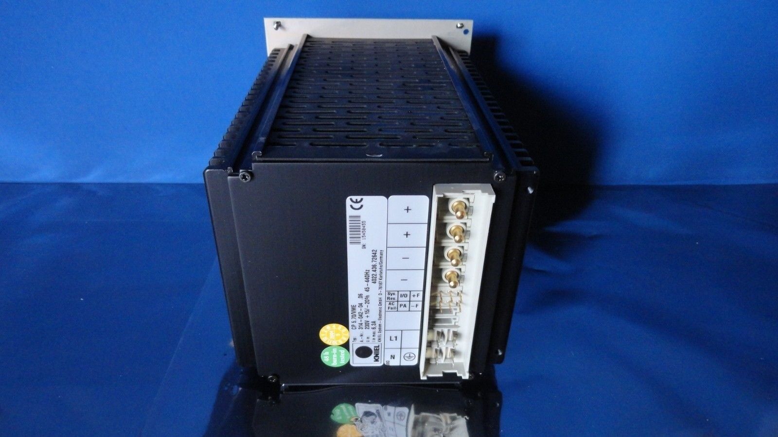
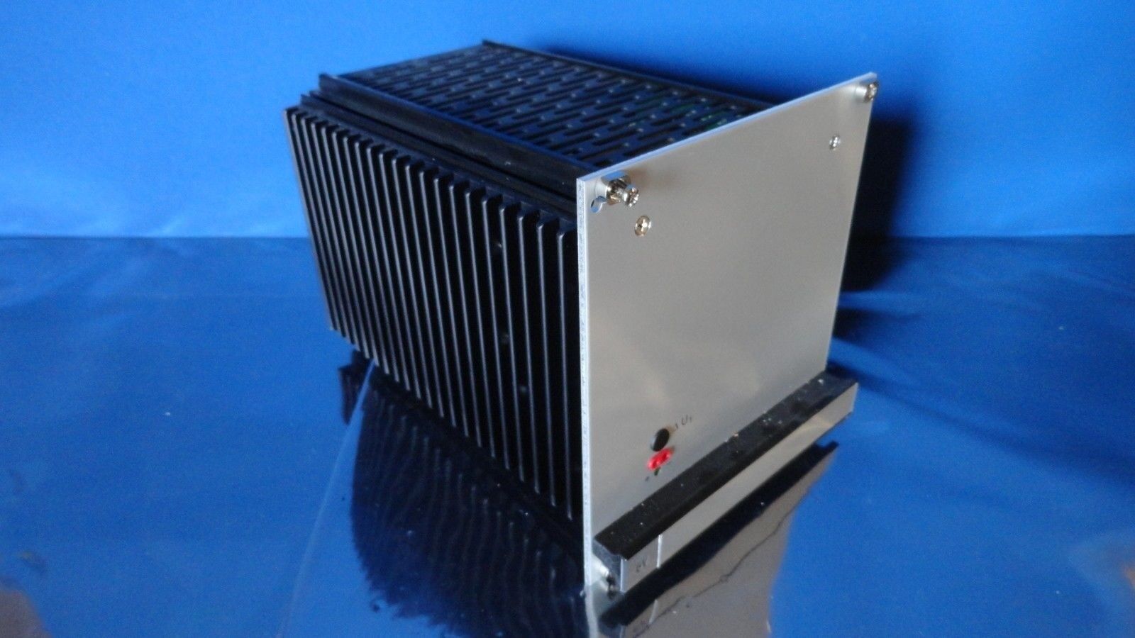
ASML 4022.436.72642是ASML极紫外(EUV)光刻机的核心晶圆传输组件,专为3nm及以下先进制程设计。其核心功能包括:
亚微米级定位精度:晶圆对准误差≤0.5μm(RMS),表面颗粒污染≤0.1μm(Class 1标准)。
超高速传输:单晶圆处理周期<8秒,产能提升30%。
真空兼容性:在1×10⁻⁶Pa真空环境下稳定运行,无油润滑设计。
产品详细说明
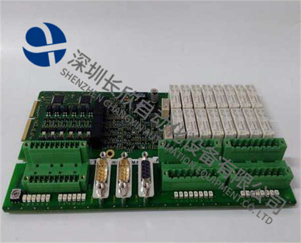
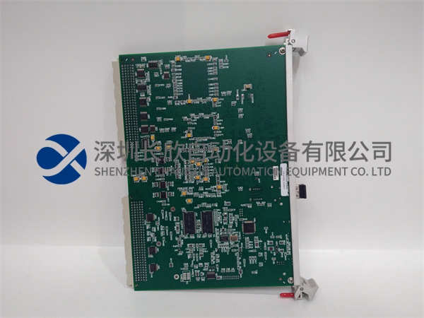
1.技术架构与创新
机械臂结构:
碳纤维复合材料:重量减轻40%,惯性矩<0.1 kg·m²。
冗余驱动系统:6自由度(X/Y/Z/θx/θy/θz)协同控制,动态响应时间<5ms。
传感与控制:
光纤激光干涉仪:分辨率≤0.1pm,抗环境振动干扰比≥60dB。
AI驱动补偿:基于机器学习的热形变预测模型,补偿精度≥99.5%。
2.工艺适配性
EUV光刻应用:
多工件台协同:支持双晶圆台交替传输,减少曝光等待时间25%。
洁净室集成:模块化设计,单次维护耗时<6小时。
特殊环境适配:
辐射耐受:可承受EUV光子流密度≥10¹⁴photons/cm²·s,表面损伤阈值>10¹⁶photons/cm²。
低温环境:在-20℃~80℃温度范围内保持定位精度。
3.行业应用案例
台积电3nm工艺:2023年导入后,晶圆产能提升20%,良率波动幅度从±2%降至±0.8%。
三星GAA晶体管制造:2024年用于逻辑芯片生产,关键层对准误差从±1.2μm降至±0.6μm。
英特尔封装技术:2025年集成后,TSV通孔良率提升18%。
技术规格:ASML 4022.436.72642
参数项规格描述
运动范围X/Y轴±200mm,Z轴±50mm
定位精度≤0.5μm(RMS)
传输速度水平移动≥600mm/s,垂直移动≥150mm/s
负载能力单晶圆承载≥100kg(含防护罩)
Product brief description
ASML 4022.436.72642 is the core wafer transmission component of ASML extreme ultraviolet(EUV)lithography machine,designed for advanced processes under 3nm and below.Its core functions include:
Submicron-level positioning accuracy:wafer alignment error≤0.5μm(RMS),surface particle contamination≤0.1μm(Class 1 standard).
Ultra-high speed transmission:single wafer processing cycle<8 seconds,production capacity increased by 30%.
Vacuum compatibility:Stable operation in 1×10⁻⁶Pa vacuum environment,oil-free lubricating design.
Product details
1.Technical Architecture and Innovation
Mechanical arm structure:
Carbon fiber composite material:40%weight reduction,moment of inertia<0.1 kg·m².
Redundant drive system:6 degrees of freedom(X/Y/Z/θx/θy/θz)coordinated control,dynamic response time<5ms.
Sensing and control:
Fiber laser interferometer:resolution≤0.1pm,anti-environmental vibration interference ratio≥60dB.
AI-driven compensation:a thermal deformation prediction model based on machine learning,with compensation accuracy of≥99.5%.
2.Process adaptability
EUV lithography applications:
Multi-workpiece platform collaboration:supports alternating transmission of dual wafer platforms,reducing exposure waiting time by 25%.
Clean room integration:modular design,single maintenance takes<6 hours.
Special environment adaptation:
Radiation tolerance:Can withstand EUV photon flow density≥10¹⁴photos/cm²·s,surface damage threshold>10¹⁶photos/cm².
Low temperature environment:maintain positioning accuracy within the temperature range of-20℃~80℃.
3.Industry application cases
TSMC’s 3nm process:After the introduction in 2023,the wafer production capacity will increase by 20%,and the yield fluctuation range will drop from±2%to±0.8%.
Samsung GAA transistor manufacturing:used for logic chip production in 2024,with the critical layer alignment error dropping from±1.2μm to±0.6μm.
Intel Packaging Technology:After integration in 2025,the yield of TSV through-holes will increase by 18%.
Technical specifications:ASML 4022.436.72642
Parameters Specification Description
Range of motion:X/Y axis±200mm,Z axis±50mm
Positioning accuracy≤0.5μm(RMS)
Transmission speed:Horizontal movement≥600mm/s,vertical movement≥150mm/s
Load capacity Single wafer bearing≥100kg(including protective cover)