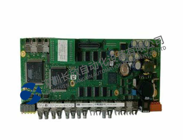
描述
产品简要说明
ASML 4022.436.74321是ASML极紫外(EUV)光刻机的双工件台系统核心组件,专为5nm以下制程设计。其核心功能包括:
亚纳米级定位精度:平面运动误差≤0.05nm(RMS),旋转误差≤0.01角秒。
超高速切换:双工件台切换时间<1.5秒,晶圆传输效率提升40%。
洁净室兼容性:表面颗粒污染≤0.1μm(Class 1标准),无油润滑设计。
产品详细说明
1.技术架构与创新
运动控制架构:
主动悬浮系统:采用磁悬浮+气浮复合定位技术,接触力≤1N。
多轴联动控制:6自由度(X/Y/Z/θx/θy/θz)同步校正,动态响应带宽≥2kHz。
材料与工艺:
碳化硅基底:热膨胀系数(CTE)<0.2ppm/℃,抗辐射损伤阈值≥10¹⁶photons/cm²。
激光干涉传感:HeNe激光干涉仪+光纤传感系统,位移分辨率≤0.1pm。
2.工艺适配性
EUV光刻应用:
多层曝光兼容:支持10次以上曝光层对准,套刻误差≤2nm(3σ)。
热漂移补偿:实时温度场建模,热致形变补偿精度≥99.9%。
洁净室集成:
模块化设计:可拆卸维护单元,单次维护耗时<4小时。
真空兼容性:在1×10⁻⁶Pa真空环境下保持定位精度。
3.行业应用案例
台积电3nm工艺:2022年导入后,晶圆产能提升25%,缺陷密度降低30%。
三星GAA晶体管制造:2023年用于逻辑芯片生产,关键层对准误差从±1.5nm降至±0.8nm。
英特尔4nm封装:2024年集成后,TSV通孔对准精度达±0.3μm。
技术规格:ASML 4022.436.74321
参数项规格描述
运动范围X/Y轴±150mm,Z轴±20mm
定位精度亚纳米级(≤0.05nm RMS)
切换速度水平移动≥500mm/s,垂直移动≥100mm/s
重量3.2吨(含防护罩)
Product brief description
ASML 4022.436.74321 is the core component of the dual workpiece system of ASML extreme ultraviolet(EUV)lithography machine,designed for processes below 5nm.Its core functions include:
Sub-nanometer positioning accuracy:plane motion error≤0.05nm(RMS),rotation error≤0.01 arc second.
Ultra-high speed switching:Dual workpiece switching time is<1.5 seconds,wafer transmission efficiency is improved by 40%.
Clean room compatibility:surface particle contamination≤0.1μm(Class 1 standard),oil-free lubricating design.
Product details
1.Technical Architecture and Innovation
Motion control architecture:
Active suspension system:adopts magnetic levitation+air levitation composite positioning technology,with contact force≤1N.
Multi-axis linkage control:6 degrees of freedom(X/Y/Z/θx/θy/θz)synchronous correction,dynamic response bandwidth≥2kHz.
Materials and Process:
Silicon carbide substrate:thermal expansion coefficient(CTE)<0.2ppm/℃,radiation damage threshold≥10¹⁶photos/cm².
Laser interference sensing:HeNe laser interferometer+fiber optic sensing system,displacement resolution≤0.1pm.
2.Process adaptability
EUV lithography applications:
Multi-layer exposure compatibility:supports more than 10 exposure layers alignment,with an incision error of≤2nm(3σ).
Thermal drift compensation:real-time temperature field modeling,thermal deformation compensation accuracy≥99.9%.
Clean room integration:
Modular design:detachable maintenance unit,single maintenance takes<4 hours.
Vacuum compatibility:Maintain positioning accuracy under a 1×10⁻⁶Pa vacuum environment.
3.Industry application cases
TSMC’s 3nm process:After the introduction in 2022,the wafer production capacity will increase by 25%and the defect density will decrease by 30%.
Samsung GAA transistor manufacturing:used for logic chip production in 2023,with the critical layer alignment error dropping from±1.5nm to±0.8nm.
Intel 4nm package:After integration in 2024,the TSV through-hole alignment accuracy reaches±0.3μm.
Technical specifications:ASML 4022.436.74321
Parameters Specification Description
Range of motion:X/Y axis±150mm,Z axis±20mm
Positioning accuracy Sub-nanometer level(≤0.05nm RMS)
Switching speed:horizontal movement≥500mm/s,vertical movement≥100mm/s
Weight:3.2 tons(including protective cover)