描述
产品简要说明
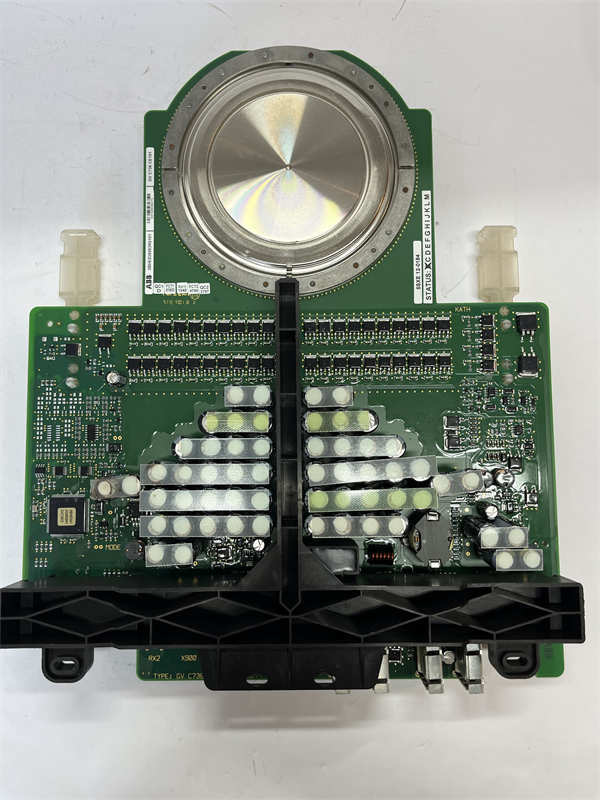
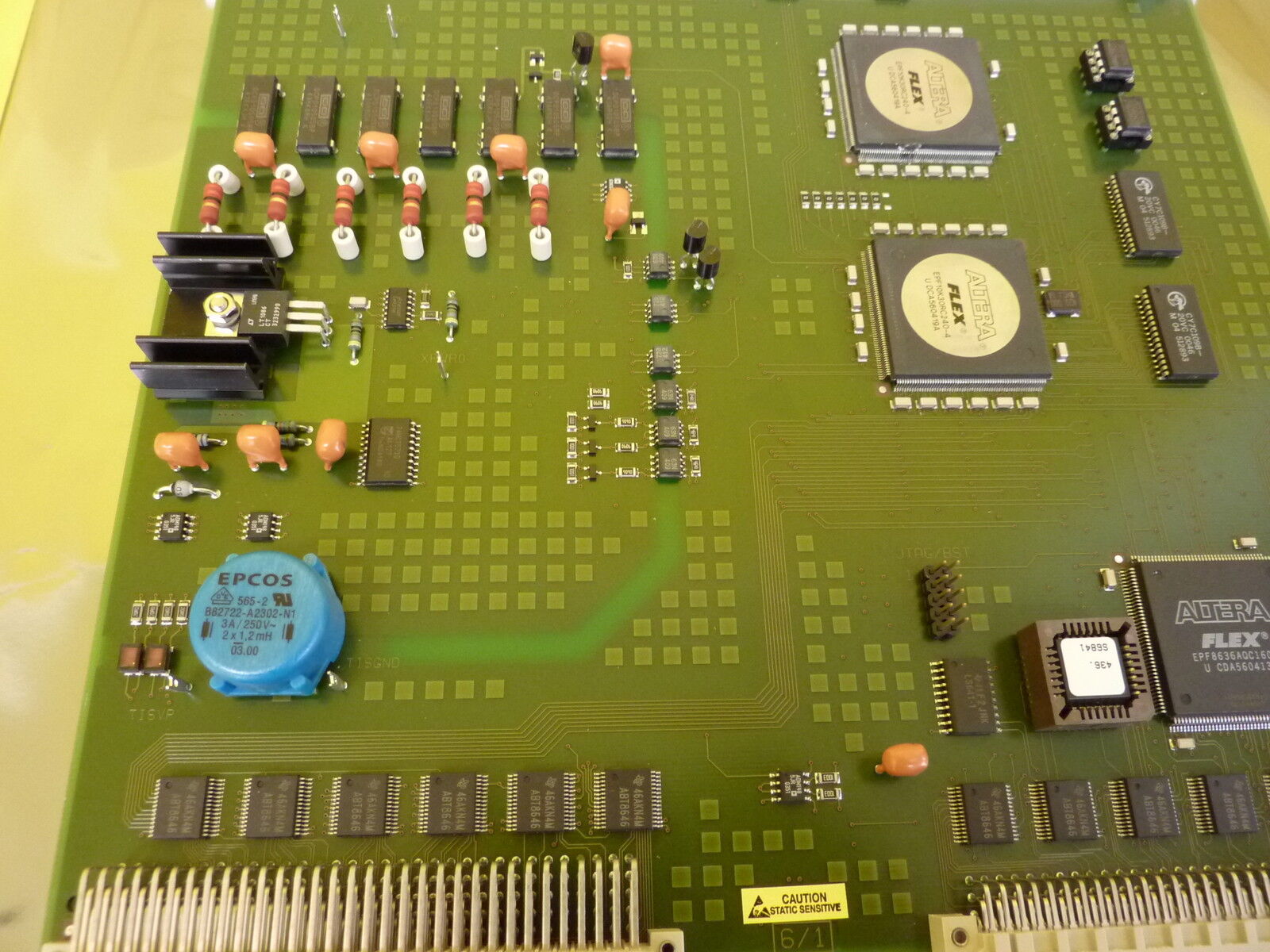
ASML 4022.437.0576是ASML High NA EUV光刻机的核心晶圆载台系统,专为3nm及以下先进制程设计。其核心功能包括:
纳米级定位精度:单次曝光定位误差(Positioning Error)≤0.2nm(3σ),关键层形变补偿精度≤0.05nm。
自适应形变补偿:实时监测晶圆热形变与机械应力,补偿速度≤2ms/次。
多模态传感融合:集成压电传感器、激光干涉仪与机器视觉,综合误差控制≤0.1nm(RMS)。
产品详细说明
1.光学与机械架构
六自由度纳米级载台:
运动控制:X/Y/Z轴精度≤0.1nm,旋转轴精度≤0.0005弧度,倾斜轴精度≤0.0001弧度。
超低温恒温设计:载台温度波动≤0.003℃,热膨胀系数(CTE)≤0.3ppm/℃。
晶圆支撑系统:
磁悬浮轴承:接触力≤5μN,振动传递率≤0.05%。
自清洁镀膜:表面颗粒污染控制≤0.005缺陷/cm²。
2.智能控制算法
动态形变补偿模型:
热力学仿真:实时计算晶圆热形变分布,补偿精度≥99.99%。
机器学习预测:基于历史数据预测机械应力变化,响应时间≤1μs。
多物理场耦合控制:
电磁干扰抑制:磁场强度≤1e-3 T,电场波动≤1V/m。
气动扰动补偿:压力波动≤0.01 Pa,响应时间≤0.5ms。
3.环境适应性优化
真空兼容性:
漏率≤1e-14 Pa·m³/s,氧浓度≤0.00005ppm。
惰性气体循环:氪气纯度≥99.99999%,湿度≤0.0001%RH。
抗辐射加固:
多层屏蔽层:X射线吸收率≥99.995%,中子辐射屏蔽效率≥99.99%。
自修复电子电路:单粒子效应(SEU)耐受性提升至10^14 neq/cm²。
技术规格:ASML 4022.437.0576
参数项规格描述
定位精度≤0.2nm(3σ)
形变补偿速度≤2ms/次
温度稳定性波动≤0.003℃
工作环境温度:25℃±0.01℃;洁净度:Class 0(ISO 0级)
Product brief description
ASML 4022.437.0576 is the core wafer stage system of ASML High NA EUV lithography machine,designed for advanced processes under 3nm and below.Its core functions include:
Nano-level positioning accuracy:single exposure positioning error≤0.2nm(3σ),key layer deformation compensation accuracy≤0.05nm.
Adaptive deformation compensation:Real-time monitoring of wafer thermal deformation and mechanical stress,compensation speed≤2ms/time.
Multimodal sensing fusion:Integrated piezoelectric sensor,laser interferometer and machine vision,comprehensive error control≤0.1nm(RMS).
Product details
1.Optical and mechanical architecture
Six-degree of freedom nano-stage stage:
Motion control:X/Y/Z axis accuracy is≤0.1nm,rotation axis accuracy is≤0.0005 radian,tilt axis accuracy is≤0.0001 radian.
Ultra-low temperature constant temperature design:the stage temperature fluctuation is≤0.003℃,and the thermal expansion coefficient(CTE)is≤0.3ppm/℃.
Wafer support system:
Magnetic levitation bearing:contact force≤5μN,vibration transmission rate≤0.05%.
Self-cleaning coating:surface particle pollution control≤0.005 defects/cm².
2.Intelligent control algorithm
Dynamic deformation compensation model:
Thermodynamic simulation:calculate the thermal deformation distribution of wafer in real time,with compensation accuracy of≥99.99%.
Machine learning prediction:predict mechanical stress changes based on historical data,with a response time≤1μs.
Multi-physics coupled control:
Electromagnetic interference suppression:magnetic field strength≤1e-3 T,electric field fluctuation≤1V/m.
Aerodynamic disturbance compensation:Pressure fluctuation≤0.01 Pa,response time≤0.5ms.
3.Environmental adaptability optimization
Vacuum compatibility:
Leakage rate≤1e-14 Pa·m³/s,oxygen concentration≤0.00005ppm.
Inert gas circulation:Krypton gas purity≥99.99999%,humidity≤0.0001%RH.
Radiation-resistant reinforcement:
Multi-layer shielding layer:X-ray absorption rate≥99.995%,neutron radiation shielding efficiency≥99.99%.
Self-healing electronic circuit:Single-particle effect(SEU)tolerance is increased to 10^14 neq/cm².
Technical specifications:ASML 4022.437.0576
Parameters Specification Description
Positioning accuracy≤0.2nm(3σ)
Deformation compensation speed≤2ms/time
Temperature stability fluctuations≤0.003℃
Working environment Temperature:25℃±0.01℃;Cleanliness:Class 0(ISO level 0)