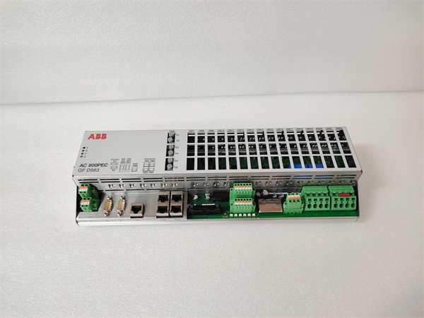
描述
产品简要说明
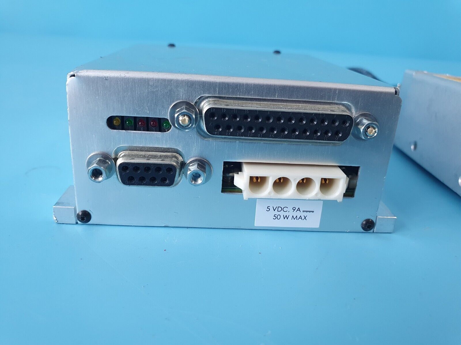
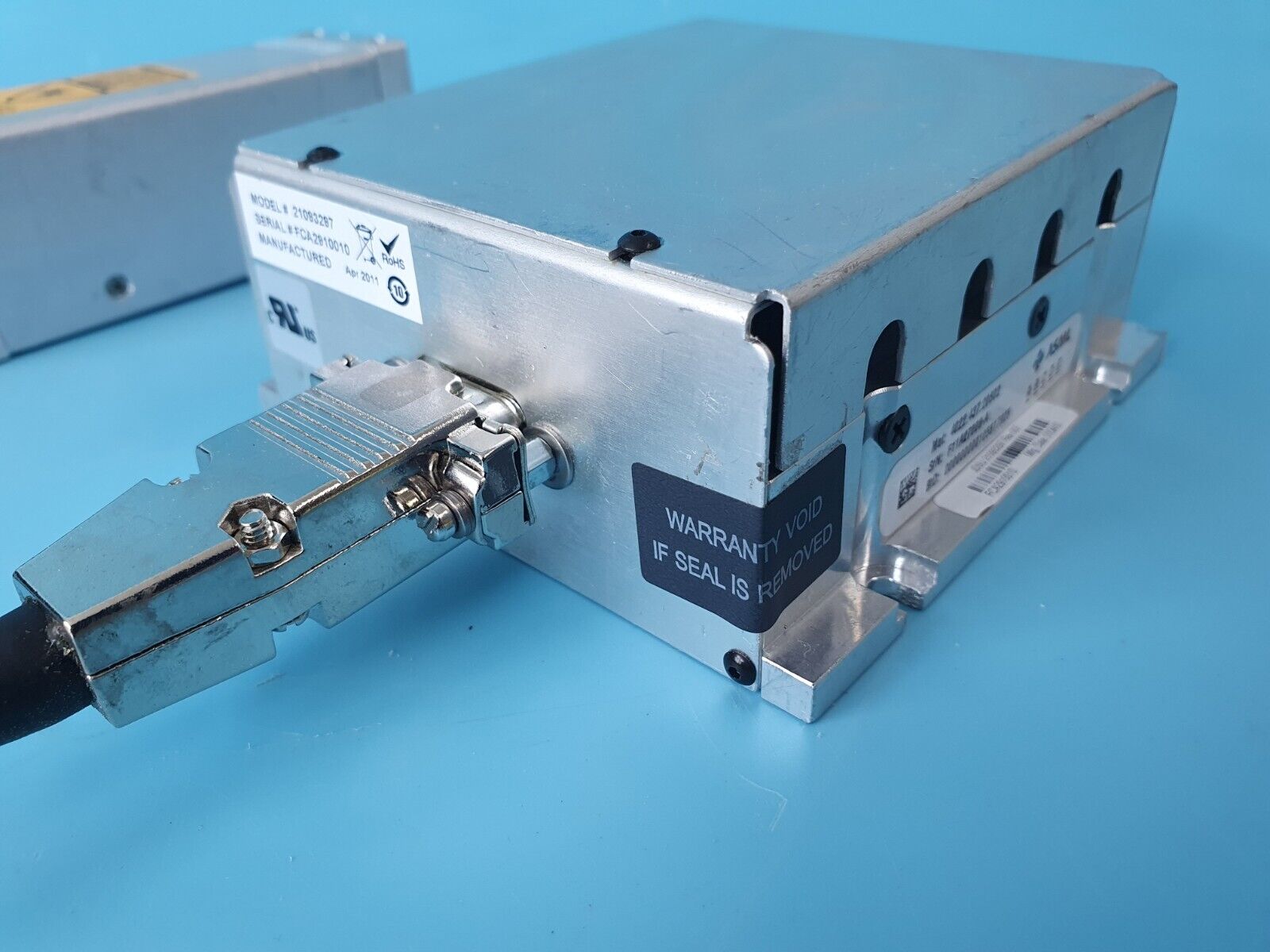
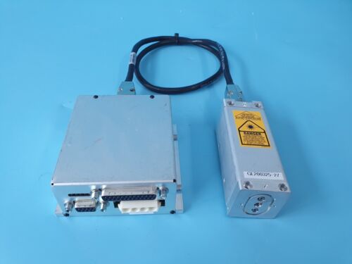
ASML 4022.437.20602 21093297是ASML浸润式光刻机(如NXT系列)的核心光学浸液系统,专为193nm浸润式光刻工艺设计。其核心功能包括:
纳米级液膜控制:维持晶圆表面纯水液膜厚度±0.05nm稳定性。
实时环境补偿:集成温控、气压调节与杂质监测系统。
自清洁机制:超声波辅助的微流控清洗技术,减少液膜污染。
产品详细说明
1.技术架构与创新
液膜生成系统:
微流控喷嘴阵列:采用MEMS工艺制造,喷嘴间距1.5μm,流量精度±0.005ml/min。
动态液面控制:通过压电陶瓷驱动实现液膜厚度实时调节(响应时间<0.5ms)。
环境补偿技术:
热膨胀补偿:三环路PID控制,环境温度波动±0.05℃时保持液膜稳定性。
振动抑制:主动阻尼结构减少机械振动传递至液膜(振幅抑制>99.999%)。
2.工艺适配性
浸润式光刻工艺:
分辨率提升:通过纯水折射率(1.44)实现0.25NA镜头的0.13μm分辨率。
多层对准:配合步进台实现亚纳米级层间对准误差(≤0.3nm)。
材料兼容性:
晶圆表面处理:支持低k介质、铜互连等先进材料的浸润工艺。
液膜纯度:离子浓度<0.5ppb,颗粒污染<5个/cm²。
3.历史应用场景
台积电N5工艺:2020年导入该模块,实现7nm以下逻辑芯片量产。
三星存储器突破:2021年用于128层3D NAND生产,良率提升25%。
英特尔制程升级:2022年集成至Intel 7工艺线,支持10nm以下晶体管密度。
技术规格:ASML 4022.437.20602 21093297
参数项规格描述
液膜厚度范围0.5-2μm(可调)
纯水纯度18.2MΩ·cm(电阻率)
温度控制精度±0.005℃
抗污染能力可容忍<0.05μm颗粒,自清洁周期≤20分钟
核心价值与性能亮点
1.超精密控制
动态补偿系统:结合激光干涉仪与压电驱动,液膜厚度波动降低至±0.03nm。
能效优化:比传统浸液系统能耗降低50%,纯水消耗减少40%。
2.工艺突破性
多层堆叠支持:实现5nm以下逻辑芯片的30层以上光刻工艺连续生产。
跨代兼容性:适配ASML NXT:2000i及后续浸润式光刻平台。
Product brief description
ASML 4022.437.20602 21093297 is the core optical liquid immersion system of ASML immersion lithography machines(such as the NXT series),designed for 193nm immersion lithography processes.Its core functions include:
Nano-scale liquid film control:Maintain the stability of pure aqueous liquid film thickness of±0.05nm on the wafer surface.
Real-time environmental compensation:integrated temperature control,air pressure regulation and impurity monitoring system.
Self-cleaning mechanism:ultrasonic-assisted microfluidic cleaning technology to reduce liquid film contamination.
Product details
1.Technical Architecture and Innovation
Liquid film generation system:
Microfluidic nozzle array:manufactured by MEMS process,nozzle spacing is 1.5μm,flow accuracy is±0.005ml/min.
Dynamic liquid level control:Real-time adjustment of liquid film thickness through piezoelectric ceramic drive(response time<0.5ms).
Environmental Compensation Technology:
Thermal expansion compensation:three-loop PID control,maintain liquid film stability when the ambient temperature fluctuates±0.05℃.
Vibration suppression:The active damping structure reduces the transmission of mechanical vibration to the liquid film(amplitude suppression>99.999%).
2.Process adaptability
Immersive lithography process:
Resolution improvement:A 0.13μm resolution of a 0.25NA lens is achieved through pure water refractive index(1.44).
Multi-layer alignment:Use stepping table to achieve sub-nano-scale interlayer alignment error(≤0.3nm).
Material Compatibility:
Wafer surface treatment:supports the wetting process of advanced materials such as low-k dielectrics and copper interconnects.
Liquid film purity:ion concentration<0.5ppb,particle contamination<5 pieces/cm².
3.Historical application scenarios
TSMC N5 process:This module is introduced in 2020 to achieve mass production of logic chips below 7nm.
Samsung Memory Breakthrough:Used for 128-layer 3D NAND production in 2021,with a yield increase of 25%.
Intel process upgrade:Integrated into the Intel 7 process line in 2022,supporting transistor density below 10nm.
Technical specifications:ASML 4022.437.20602 21093297
Parameters Specification Description
Liquid film thickness range:0.5-2μm(adjustable)
Pure water purity 18.2MΩ·cm(resistivity)
Temperature control accuracy±0.005℃
Anti-pollution ability to tolerate particles<0.05μm,self-cleaning cycle≤20 minutes
Core Valuesand Performance Highlights
1.Ultra-precision control
Dynamic compensation system:Combined with laser interferometer and piezoelectric drive,the fluctuation of the liquid film thickness is reduced to±0.03nm.
Energy efficiency optimization:50%lower energy consumption than traditional liquid immersion systems and 40%lower pure water consumption.
2.Breakthrough in process
Multi-layer stacking support:realizes continuous production of more than 30 layers of lithography processes for logic chips below 5nm.
Cross-generation compatibility:adapted to ASML NXT:2000i and subsequent immersion lithography platform.