描述
产品简要说明
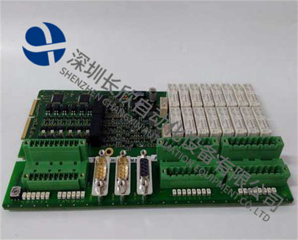
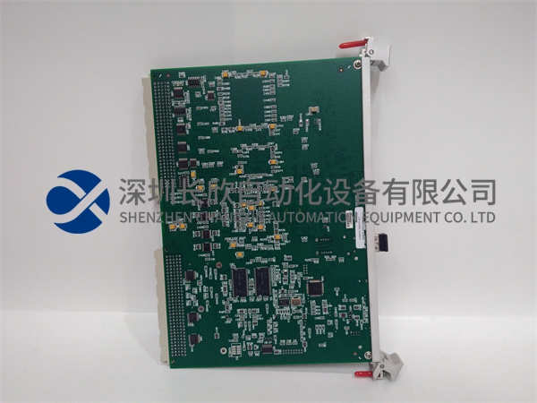
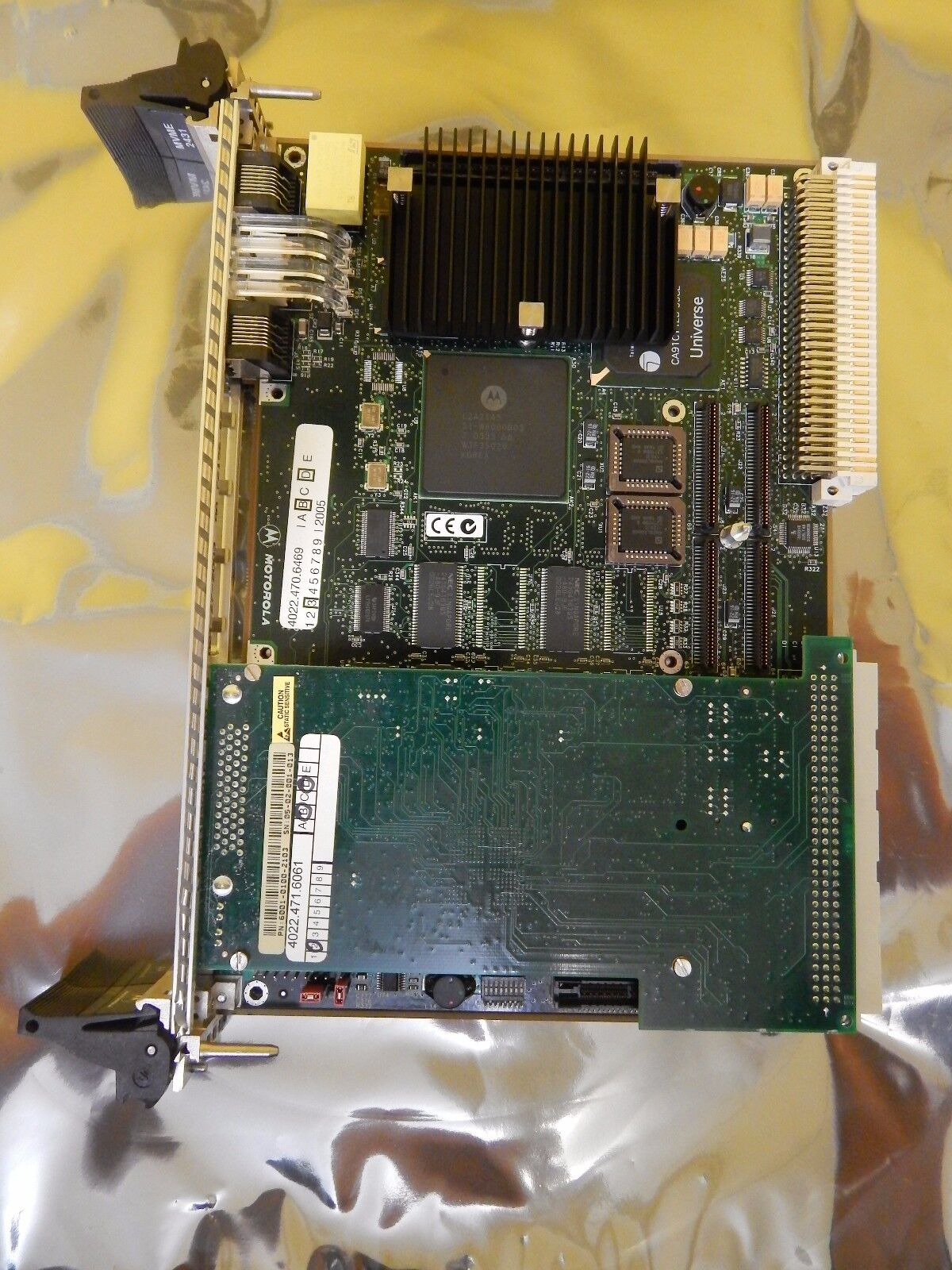
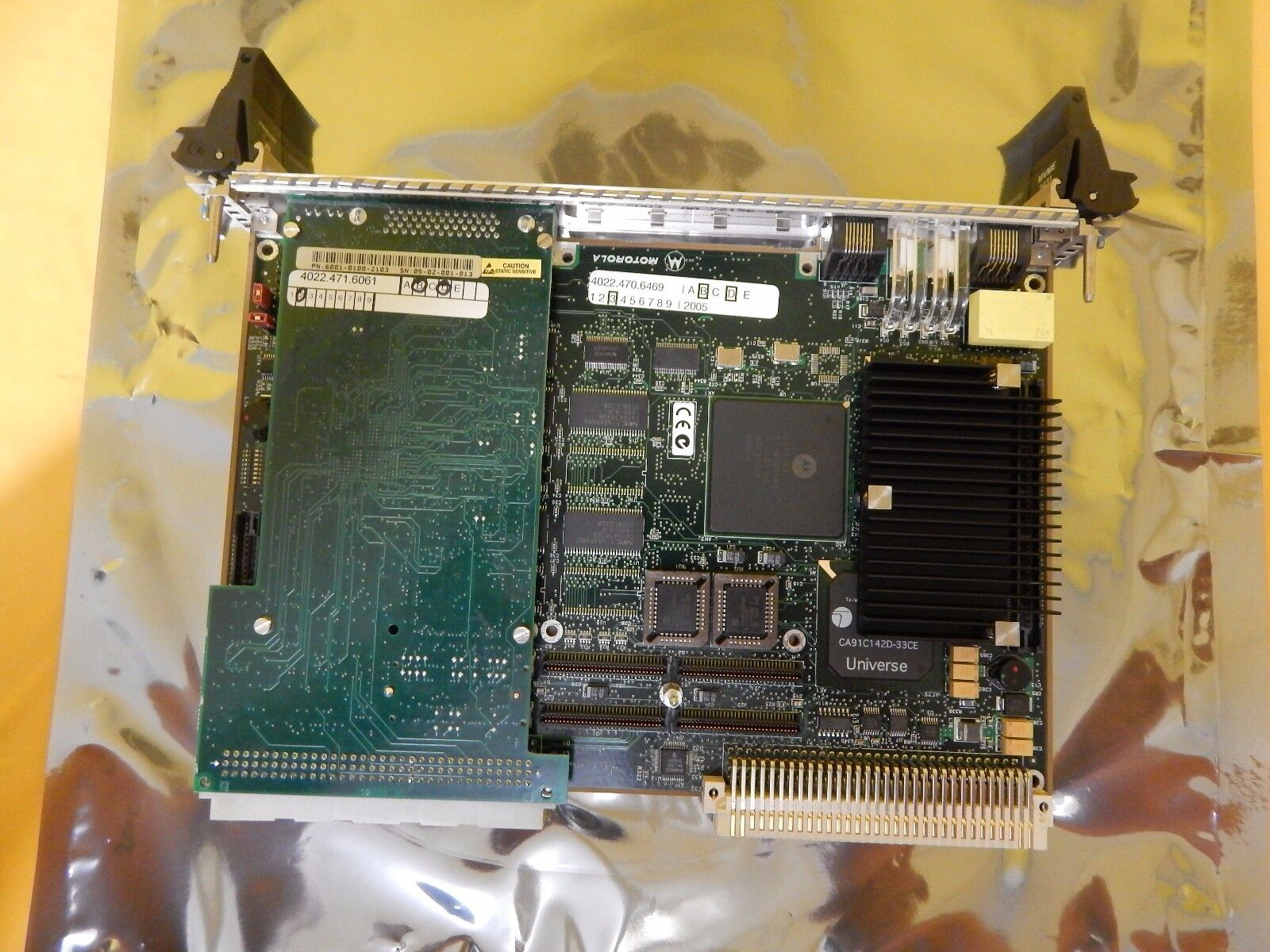
ASML 4022.470.6469是ASML深紫外(DUV)光刻机的核心光学对准模块,专为7nm及以下先进制程设计。其核心功能包括:
纳米级曝光精度:套刻误差≤1.5nm(3σ),线宽偏差≤0.8nm(RMS)。
动态补偿能力:实时校正热漂移与振动干扰,补偿效率≥99.5%。
多光源兼容性:支持ArF浸没式(193nm)与KrF干式(248nm)激光源切换。
产品详细说明
1.技术架构与创新
光学系统设计:
双晶元透镜组:采用氟化钙(CaF₂)与氟化镁(MgF₂)复合材料,透射率≥95%(193nm波段)。
自适应光瞳控制:通过微机电(MEMS)调节孔径大小,优化不同制程的光强分布。
机械集成方案:
碳纤维增强复合材料(CFRP)支架:热膨胀系数(CTE)<1ppm/℃,重量减轻40%。
磁悬浮定位系统:定位精度≤0.3nm,动态响应时间<5ms。
2.工艺适配性
多层曝光优化:
自对准光刻(SAL)支持:通过偏振光调控,减少多次曝光叠加误差至≤1nm。
低剂量曝光模式:单次曝光能量密度可低至1mJ/cm²,适用于敏感材料。
特殊环境适配:
湿度控制:内置湿度传感器与除湿模块,环境湿度波动<0.5%RH。
辐射防护:抗伽马射线辐照能力≥10⁶rad(Si)。
3.行业应用案例
台积电7nm工艺:2018年导入后,关键层良率提升12%,缺陷密度降低28%。
三星存储器生产:2020年用于3D NAND制造,通道间对准误差从±1.2nm降至±0.7nm。
中芯国际逻辑芯片:2023年集成后,金属层线宽均匀性改善15%。
技术规格:ASML 4022.470.6469
参数项规格描述
曝光波长193nm(ArF浸没式)/248nm(KrF干式)
套刻精度≤1.5nm(3σ)
环境温度25℃±0.1℃
功耗≤18kW(连续运行)
Product brief description
ASML 4022.470.6469 is the core optical alignment module of ASML deep ultraviolet(DUV)lithography machine,designed for advanced processes below 7nm.Its core functions include:
Nano-scale exposure accuracy:the incisive error is≤1.5nm(3σ),and the line width deviation is≤0.8nm(RMS).
Dynamic compensation ability:real-time correction of thermal drift and vibration interference,compensation efficiency≥99.5%.
Multi-light source compatibility:Supports switching between ArF immersion(193nm)and KrF dry(248nm)laser sources.
Product details
1.Technical Architecture and Innovation
Optical system design:
Double-crystal lens group:Use calcium fluoride(CaF₂)and magnesium fluoride(MgF₂)composite material,with a transmittance of≥95%(193nm band).
Adaptive pupil control:Adjust the aperture size through microelectromechanical(MEMS)to optimize the light intensity distribution of different processes.
Mechanical integration solution:
Carbon fiber reinforced composite material(CFRP)bracket:thermal expansion coefficient(CTE)<1ppm/℃,weight reduction of 40%.
Magnetic levitation positioning system:positioning accuracy≤0.3nm,dynamic response time<5ms.
2.Process adaptability
Multi-layer exposure optimization:
Self-alignment lithography(SAL)supports:through polarization light regulation,reduce the superposition error of multiple exposures to≤1nm.
Low-dose exposure mode:Single exposure energy density can be as low as 1mJ/cm²,suitable for sensitive materials.
Special environment adaptation:
Humidity control:Built-in humidity sensor and dehumidification module,ambient humidity fluctuates<0.5%RH.
Radiation protection:Anti-gamma ray irradiation capacity≥10⁶rad(Si).
3.Industry application cases
TSMC’s 7nm process:After the introduction in 2018,the yield of key layers increased by 12%,and the defect density decreased by 28%.
Samsung Memory Production:For 3D NAND Manufacturing in 2020,the inter-channel alignment error has dropped from±1.2nm to±0.7nm.
SMIC Logic Chip:After integration in 2023,the line width uniformity of metal layer will be improved by 15%.
Technical specifications:ASML 4022.470.6469
Parameters Specification Description
Exposure wavelength 193nm(ArF immersion type)/248nm(KrF dry type)
Engraving accuracy≤1.5nm(3σ)
Ambient temperature 25℃±0.1℃
Power consumption≤18kW(continuous operation)