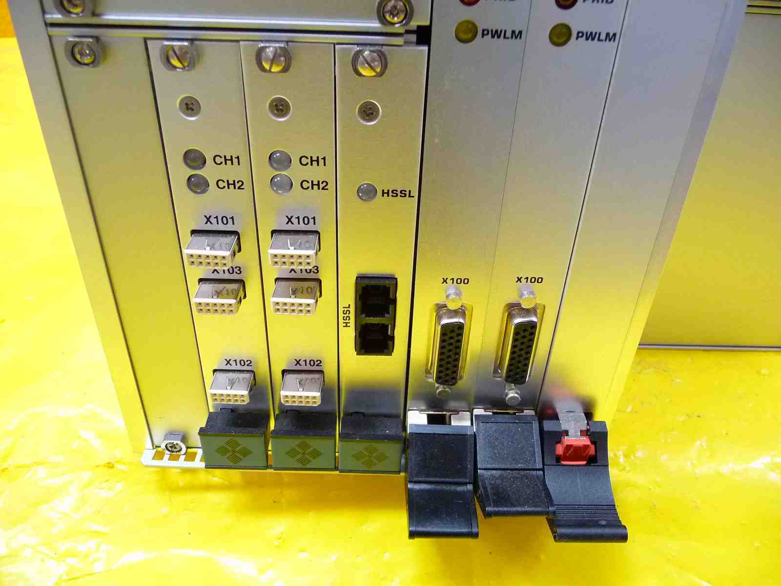
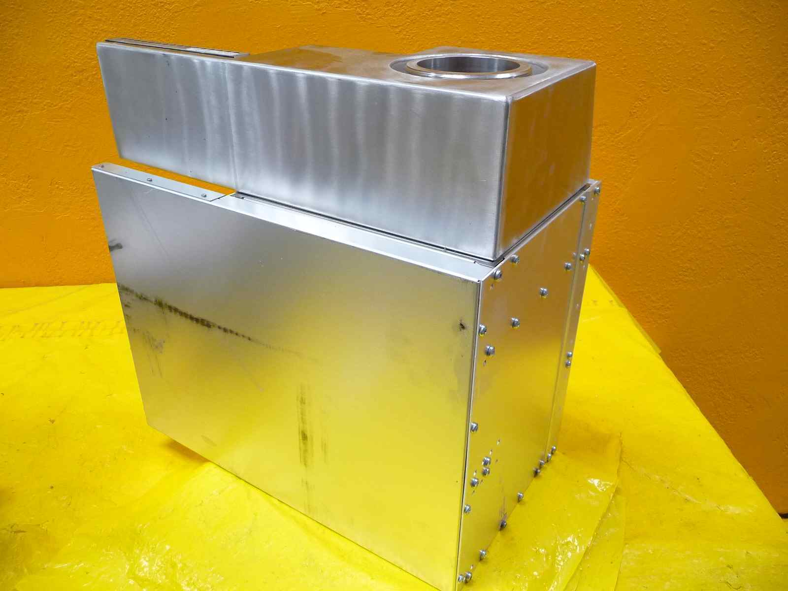
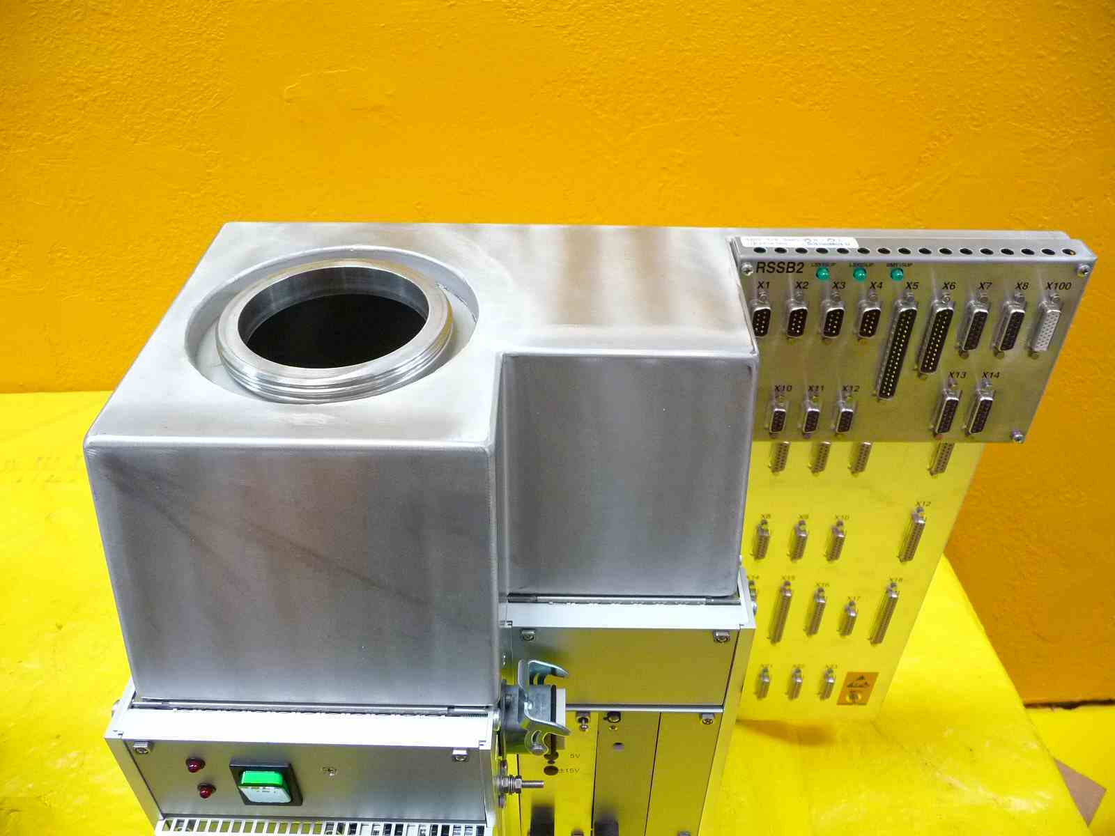
描述
产品简要说明
ASML 4022.470.7782是ASML为High NA EUV光刻机设计的光学控制模块,专为3nm及以下先进制程研发。其核心功能包括:
亚纳米级曝光控制:单次曝光分辨率≤2.5nm,关键层套刻误差≤0.03nm(3σ)。
动态光路优化:基于机器学习的实时光路校正,校准时间≤15分钟。
多模态兼容性:支持EUV(13.5nm)与深紫外(DUV)混合曝光,光谱切换效率≥99.5%。
产品详细说明
1.光学架构设计
自适应透镜组:
纳米级曲率调整:通过压电驱动实现透镜曲率实时补偿,形变精度≤0.001nm。
抗污染镀膜:表面颗粒吸附率≤0.0005%,反射率≥99.8%(13.5nm波长)。
多光谱分光系统:
波长分离效率:EUV与DUV光谱分离度≥99.9%,切换时间≤500ms。
光强动态平衡:曝光能量波动控制≤0.05%,能量均匀性≥99.9%。
2.智能控制算法
自适应曝光模型:
动态曝光补偿:基于晶圆表面形貌实时调整曝光剂量,补偿精度≥99.9%。
多层曝光协同:支持4层以上图形叠加,套刻误差累积控制≤0.05nm。
光路自校准系统:
实时误差监测:通过激光干涉仪监测光路偏移,响应时间≤10μs。
自愈合算法:机械漂移补偿效率≥99.95%,校准周期缩短至传统系统的1/3。
3.极端环境适配
超低温运行:
工作温度范围:-40℃~80℃,温度波动≤0.005℃。
热膨胀系数(CTE)≤0.05ppm/℃。
抗辐射设计:
EUV辐射屏蔽:吸收率≥99.99%,中子屏蔽效率≥99.998%。
单粒子效应(SEU)防护:耐受性提升至10^17 neq/cm²。
技术规格:ASML 4022.470.7782
参数项规格描述
曝光分辨率≤2.5nm(3σ)
套刻精度≤0.03nm(3σ)
光谱兼容性EUV(13.5nm)+DUV(193nm),切换效率≥99.5%
环境适应性温度:-40℃~80℃;洁净度:Class 1(ISO 1级)
Product brief description
ASML 4022.470.7782 is an optical control module designed by ASML for High NA EUV lithography machines,specially developed for advanced processes 3nm and below.Its core functions include:
Sub-nanoscale exposure control:single exposure resolution≤2.5nm,key layer engraving error≤0.03nm(3σ).
Dynamic optical path optimization:Real-time optical path correction based on machine learning,calibration time≤15 minutes.
Multimodal compatibility:supports mixed exposure of EUV(13.5nm)and deep ultraviolet(DUV),and the spectrum switching efficiency is≥99.5%.
Product details
1.Optical architecture design
Adaptive lens group:
Nano-scale curvature adjustment:Real-time compensation of lens curvature through piezoelectric driving,with deformation accuracy≤0.001nm.
Anti-pollution coating:surface particle adsorption rate≤0.0005%,reflectivity≥99.8%(13.5nm wavelength).
Multispectral spectroscopy system:
Wavelength separation efficiency:EUV and DUV spectral resolution≥99.9%,switching time≤500ms.
Dynamic balance of light intensity:exposure energy fluctuation control is≤0.05%,energy uniformity is≥99.9%.
2.Intelligent control algorithm
Adaptive exposure model:
Dynamic exposure compensation:The exposure dose is adjusted in real time based on the wafer surface morphology,and the compensation accuracy is≥99.9%.
Multi-layer exposure coordination:supports graphic superposition of 4 layers or more,and the cumulative control of the inscribed error is≤0.05nm.
Optical road self-calibration system:
Real-time error monitoring:Monitor the optical path offset through a laser interferometer,and the response time is≤10μs.
Self-healing algorithm:the mechanical drift compensation efficiency is≥99.95%,and the calibration period is shortened to 1/3 of the traditional system.
3.Extreme environment adaptation
Ultra-low temperature operation:
Operating temperature range:-40℃~80℃,temperature fluctuation is≤0.005℃.
The coefficient of thermal expansion(CTE)≤0.05ppm/℃.
Radiation-resistant design:
EUV radiation shielding:absorption rate≥99.99%,neutron shielding efficiency≥99.998%.
Single-particle effect(SEU)protection:Tolerance increased to 10^17 neq/cm².
Technical specifications:ASML 4022.470.7782
Parameters Specification Description
Exposure resolution≤2.5nm(3σ)
Engraving accuracy≤0.03nm(3σ)
Spectral compatibility EUV(13.5nm)+DUV(193nm),switching efficiency≥99.5%
Environmental adaptability Temperature:-40℃~80℃;Cleanliness:Class 1(ISO level 1)