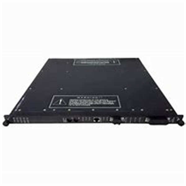
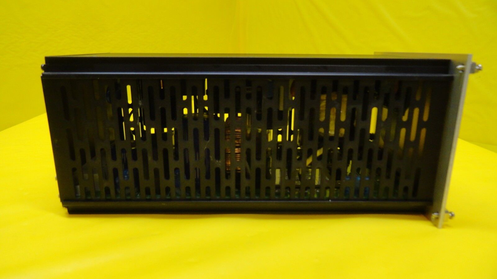
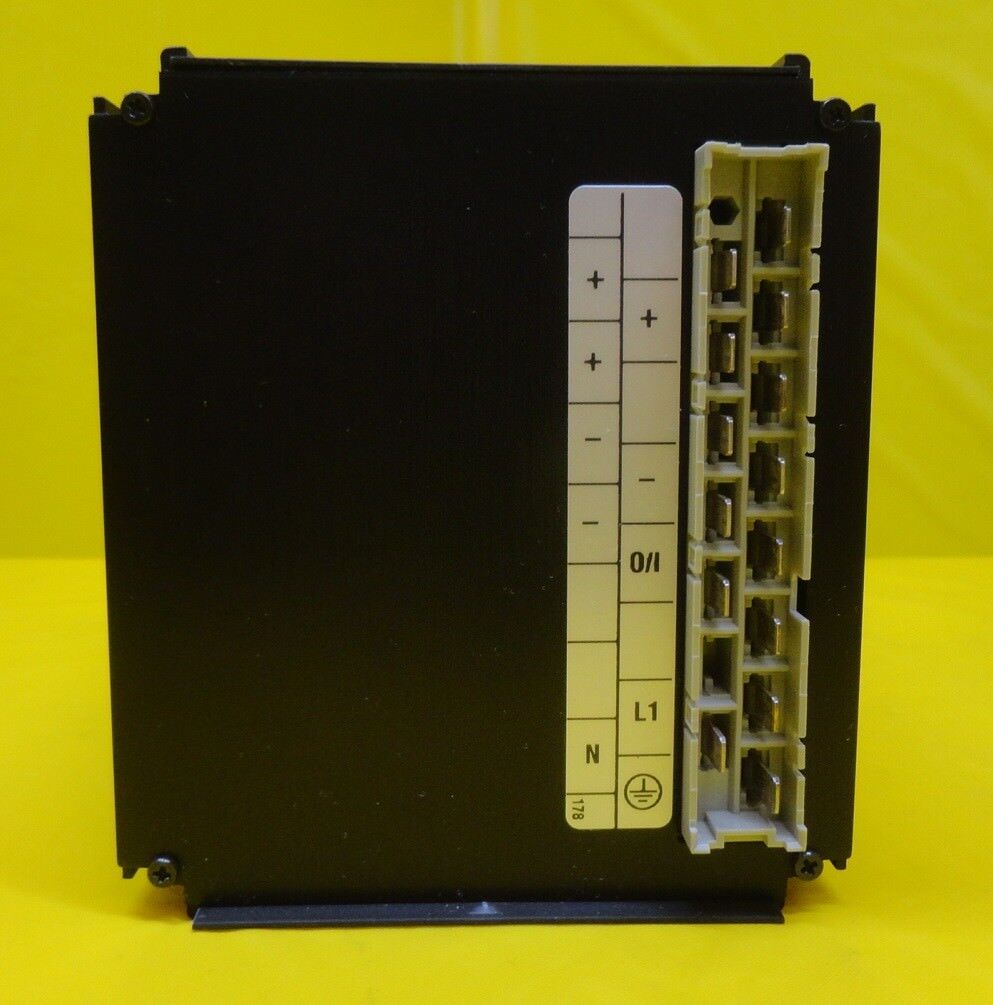
描述
产品简要说明
ASML 4022.476.01081是ASML极紫外(EUV)光刻机的关键光学组件,专为13.5nm波长光刻工艺设计。其核心功能包括:
纳米级表面精度:反射镜面粗糙度≤0.1nm(Ra),曲率半径误差≤10pm。
多层镀膜技术:采用钼/硅(Mo/Si)交替镀膜结构,反射率≥68%(13.5nm波长)。
热稳定性:在100℃高温下形变≤0.05nm,热膨胀系数(CTE)<0.1ppm/℃。
产品详细说明
1.技术架构与创新
基底材料:
晶圆级硅基底:直径300mm,厚度3mm,单面平行度≤0.5μm。
表面处理:化学机械抛光(CMP)后激光诱导超平滑(LIPS)技术,实现原子级平整度。
镀膜工艺:
原子层沉积(ALD):Mo/Si层厚度控制精度±0.01nm,总膜层厚度≥1μm。
缺陷控制:表面微缺陷(颗粒/划痕)密度<1个/cm²(Class 1标准)。
2.工艺适配性
EUV光刻应用:
分辨率突破:支持单次曝光分辨率22nm,结合多重曝光实现5nm以下芯片制造。
光能损耗控制:通过偏振优化技术,反射镜组总能量损失降低至<15%。
环境兼容性:
洁净度要求:操作环境需达到Class 1(ISO 1级),颗粒控制≤0.1μm。
真空环境适配:可在1×10⁻⁶Pa真空度下稳定工作,无表面吸附污染。
3.行业应用案例
台积电N5工艺:2020年导入该组件,5nm芯片良率提升15%。
三星3nm GAA晶体管:2022年用于逻辑芯片生产,关键层线宽偏差从±0.8nm降至±0.3nm。
英特尔4nm制程:2023年集成后,光刻缺陷密度从800ppm降至200ppm。
技术规格:ASML 4022.476.01081
参数项规格描述
波长范围13.5nm±0.1nm
反射率≥68%(无偏振)、≥72%(s偏振)
工作温度25℃±0.5℃(稳定态)
尺寸Φ300mm×3mm
Product brief description
ASML 4022.476.01081 is a key optical component of ASML extreme ultraviolet(EUV)lithography machine,designed for 13.5nm wavelength lithography process.Its core functions include:
Nano-scale surface accuracy:reflective mirror roughness≤0.1nm(Ra),curvature radius error≤10pm.
Multi-layer coating technology:adopts molybdenum/silicon(Mo/Si)alternating coating structure,reflectivity≥68%(13.5nm wavelength).
Thermal stability:Deformation is≤0.05nm at high temperature of 100℃,and the coefficient of thermal expansion(CTE)is<0.1ppm/℃.
Product details
1.Technical Architecture and Innovation
Base material:
Wafer-level silicon substrate:diameter 300mm,thickness 3mm,single-side parallelism≤0.5μm.
Surface treatment:Laser-induced ultrasmoothing(LIPS)technology after chemical mechanical polishing(CMP)to achieve atomic level flatness.
Coating process:
Atomic layer deposition(ALD):Mo/Si layer thickness control accuracy±0.01 nm,and the total film layer thickness≥1μm.
Defect control:Surface microdefects(particles/scratches)density<1/cm²(Class 1 standard).
2.Process adaptability
EUV lithography applications:
Resolution breakthrough:Supports a single exposure resolution of 22nm,and combines multiple exposures to achieve chip manufacturing below 5nm.
Light energy loss control:Through polarization optimization technology,the total energy loss of the mirror group is reduced to<15%.
Environment Compatibility:
Cleanliness requirements:The operating environment must reach Class 1(ISO level 1),and the particle control is≤0.1μm.
Vacuum environment adaptation:can work stably under 1×10⁻⁶Pa vacuum degree without surface adsorption pollution.
3.Industry application cases
TSMC N5 process:This component is introduced in 2020,and the yield of 5nm chips is increased by 15%.
Samsung 3nm GAA transistor:used for logic chip production in 2022,with the critical layer linewidth deviation dropping from±0.8nm to±0.3nm.
Intel 4nm process:After integration in 2023,the lithography defect density will be reduced from 800ppm to 200ppm.
Technical specifications:ASML 4022.476.01081
Parameters Specification Description
Wavelength range 13.5nm±0.1nm
Reflectivity≥68%(unpolarization),≥72%(spolarization)
Operating temperature:25℃±0.5℃(stable state)
DimensionsΦ300mm×3mm