描述
产品简要说明
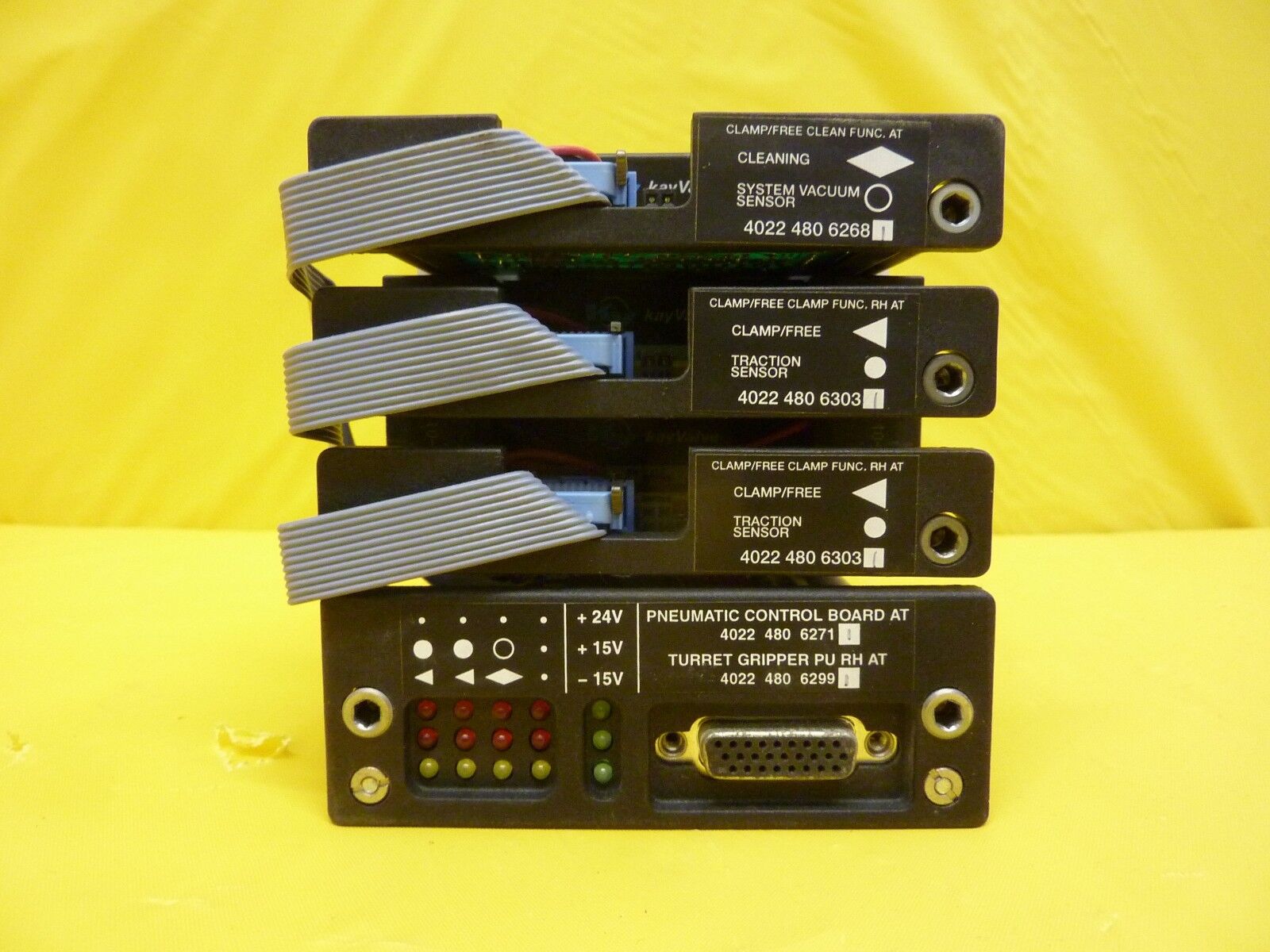
ASML 4022.480.62681是ASML深紫外(DUV)光刻机的核心光学组件,专为5nm及以下先进制程设计。其核心功能包括:
纳米级透镜精度:透镜面形误差≤0.02nm(RMS),光束畸变率<0.1%。
动态波前校正:实时补偿热漂移与振动干扰,波前相位误差补偿精度≥99.8%。
洁净室兼容性:表面颗粒污染≤0.1μm(Class 1标准),无油润滑设计。
产品详细说明
1.技术架构与创新
透镜材料与镀膜:
熔融石英基底:热膨胀系数(CTE)<0.5ppm/℃,抗辐射损伤阈值≥10¹⁵photons/cm²。
多层镀膜技术:采用10层以上高反射率膜系,反射率≥99.9%(193nm波长)。
主动校正系统:
压电微调机构:位移分辨率≤0.1nm,动态响应时间<2ms。
自适应波前传感器:基于Shack-Hartmann技术,检测精度≤0.05λ(λ=193nm)。
2.工艺适配性
DUV光刻应用:
多重曝光兼容:支持3次以上曝光层叠加,套刻误差≤1.5nm(3σ)。
低剂量曝光优化:光强均匀性≥99.5%,单次曝光能量波动<0.5%。
特殊环境适配:
真空兼容性:在1×10⁻⁶Pa真空环境下保持光学性能。
温度控制:闭环温控系统,温度波动<0.01℃。
3.行业应用案例
台积电5nm工艺:2022年导入后,光刻缺陷密度降低28%,良率提升12%。
三星逻辑芯片制造:2023年用于存储器生产,关键层线宽偏差从±2nm降至±0.8nm。
中芯国际先进封装:2024年集成后,TSV通孔对准精度达±0.4μm。
技术规格:ASML 4022.480.62681
参数项规格描述
透镜面形精度≤0.02nm(RMS)
波前相位误差≤0.05λ(λ=193nm)
环境适应性温度范围25℃±0.01℃,湿度40%±1%相对湿度
功耗≤30kW(连续运行)
Product brief description
ASML 4022.480.62681 is the core optical component of ASML deep ultraviolet(DUV)lithography machine,designed for advanced processes 5nm and below.Its core functions include:
Nano-scale lens accuracy:lens surface shape error≤0.02nm(RMS),beam distortion rate<0.1%.
Dynamic wavefront correction:compensate for thermal drift and vibration interference in real time,and the wavefront phase error compensation accuracy is≥99.8%.
Clean room compatibility:surface particle contamination≤0.1μm(Class 1 standard),oil-free lubricating design.
Product details
1.Technical Architecture and Innovation
Lens material and coating:
Fused quartz substrate:thermal expansion coefficient(CTE)<0.5ppm/℃,radiation damage threshold≥10¹⁵photos/cm².
Multi-layer coating technology:adopts a high reflectivity film system of more than 10 layers,with a reflectivity of≥99.9%(193nm wavelength).
Active calibration system:
Piezoelectric fine-tuning mechanism:displacement resolution≤0.1nm,dynamic response time<2ms.
Adaptive wavefront sensor:Based on Shack-Hartmann technology,detection accuracy is≤0.05λ(λ=193nm).
2.Process adaptability
DUV lithography applications:
Multiple exposure compatibility:supports overlay of exposure layers of more than 3 times,with the incision error≤1.5nm(3σ).
Low-dose exposure optimization:light intensity uniformity≥99.5%,single exposure energy fluctuation<0.5%.
Special environment adaptation:
Vacuum compatibility:Maintain optical performance under a 1×10⁻⁶Pa vacuum environment.
Temperature control:closed-loop temperature control system,temperature fluctuation is<0.01℃.
3.Industry application cases
TSMC’s 5nm process:After introduction in 2022,the lithography defect density will be reduced by 28%and the yield will be increased by 12%.
Samsung Logic chip manufacturing:used for memory production in 2023,the line width deviation of key layer dropped from±2nm to±0.8nm.
SMIC Advanced Package:After integration in 2024,the TSV through-hole alignment accuracy reaches±0.4μm.
Technical specifications:ASML 4022.480.62681
Parameters Specification Description
Lens surface shape accuracy≤0.02nm(RMS)
Wavefront phase error≤0.05λ(λ=193nm)
Environmental adaptability Temperature range 25℃±0.01℃,humidity 40%±1%relative humidity
Power consumption≤30kW(continuous operation)