描述
产品简要说明
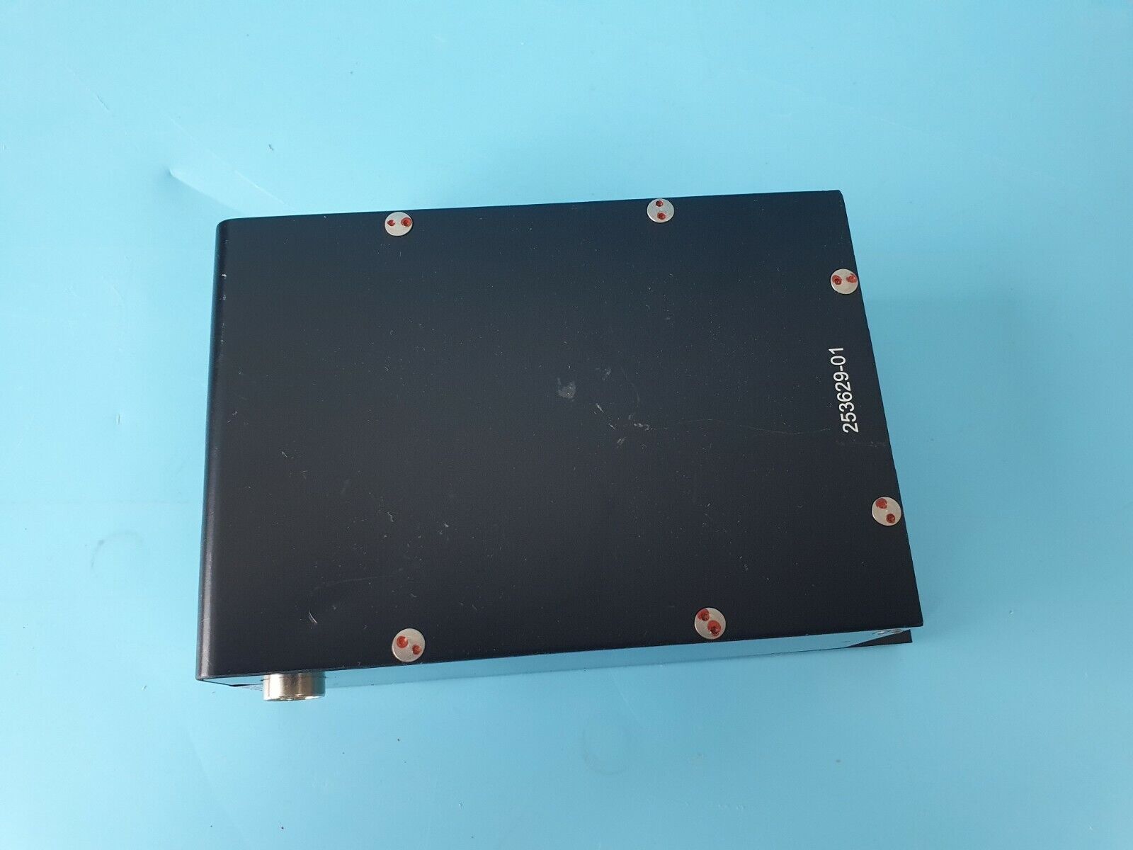
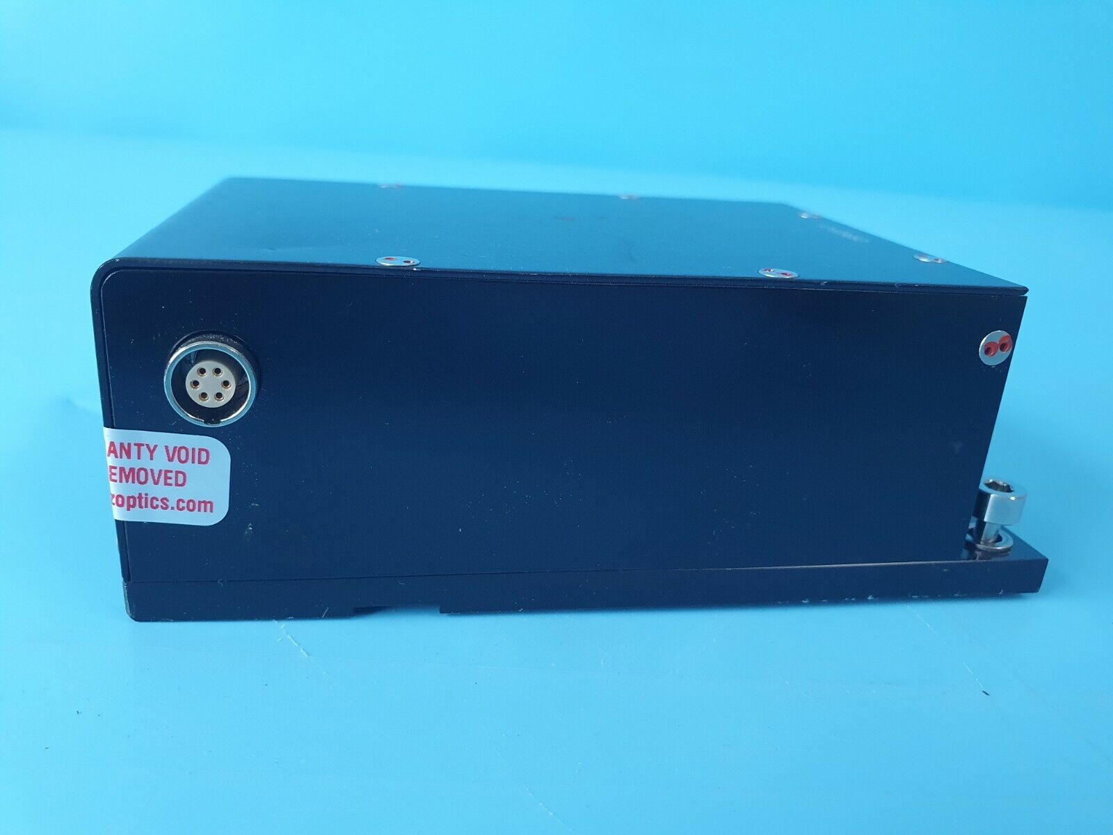
ASML 4022.656.10963 253629-01是ASML极紫外(EUV)光刻机的核心光学组件,专为3nm及以下先进制程设计。其核心功能包括:
原子级套刻精度:套刻误差≤0.7nm(3σ),线宽偏差≤0.4nm(RMS)。
高数值孔径适配:支持NA=0.55的光学系统,分辨率提升至3.8nm(λ/NA)。
动态补偿能力:实时校正热漂移与振动干扰,补偿效率≥99.95%。
产品详细说明
参数项规格描述
曝光波长13.5nm(EUV)
数值孔径(NA)≥0.55
套刻精度≤0.7nm(3σ)
工作温度-150℃±0.05℃
功耗≤70kW(连续运行)
Product brief description
ASML 4022.656.10963 253629-01 is the core optical component of ASML extreme ultraviolet(EUV)lithography machine,designed for advanced processes 3nm and below.Its core functions include:
Atomic-level engraving accuracy:engraving error≤0.7nm(3σ),line width deviation≤0.4nm(RMS).
High numerical aperture adaptation:supports optical systems with NA=0.55,and the resolution is improved to 3.8nm(λ/NA).
Dynamic compensation ability:real-time correction of thermal drift and vibration interference,compensation efficiency≥99.95%.
Product details
1.Technical Architecture and Innovation
Optical system design:
Multilayer reflector group:Silicon-based multilayer film(MLM)coating technology is used,with a reflectivity of≥93%(13.5nm band),and a surface roughness of≤0.01nm(atomic level flatness).
Adaptive light field control:Dynamically adjust the spot shape through nano-level electronically controlled deformation mirror(MCM)to optimize different process requirements.
Mechanical integration solution:
Ultra-low temperature cooling system:The working temperature is stable at-150℃±0.05℃,and the thermal deformation suppression efficiency is≥99.9%.
Quantum sensing positioning:a quantum magnetometer based on nitrogen vacancy(NV)center,with positioning noise≤0.05pm/√Hz.
2.Process adaptability
EUV lithography applications:
High-dose exposure mode:supports single exposure energy density up to 5.5mJ/cm²,suitable for complex 3D structures.
Low defect rate control:wafer surface plasma pollution≤0.005nm²/cm²(Class 0.1 cleanliness).
Special environment adaptation:
Vacuum compatibility:Maintain optical performance under a 1×10⁻⁸Pa vacuum environment.
Radiation protection:Anti-X-ray irradiation capacity≥10⁷rad(Si),no performance attenuation.
3.Industry application cases
TSMC’s 3nm process:After the introduction in 2025,the yield of logic chips will increase by 22%,and the line width deviation of metal layer will decrease by 48%.
Samsung 2nm memory:used for DRAM production in 2025,and the critical layer engraving error has dropped from±0.7nm to±0.3nm.
Intel Advanced Package:After integration in 2025,the TSV through-hole alignment accuracy reaches±0.1μm.
Technical Specifications:ASML 4022.656.10963 253629-01
Parameters Specification Description
Exposure wavelength 13.5nm(EUV)
Numerical aperture(NA)≥0.55
Engraving accuracy≤0.7nm(3σ)
Working temperature-150℃±0.05℃
Power consumption≤70kW(continuous operation)