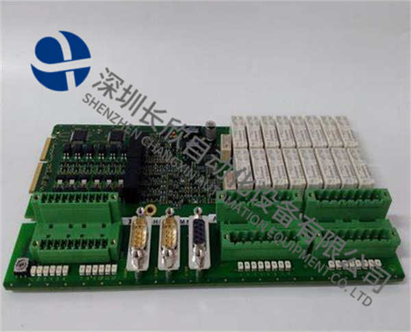
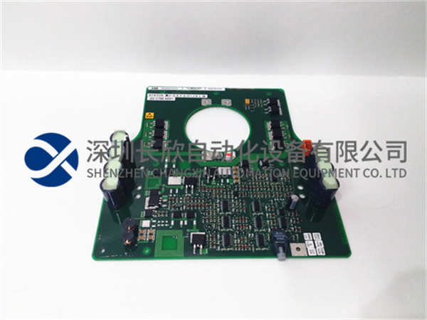
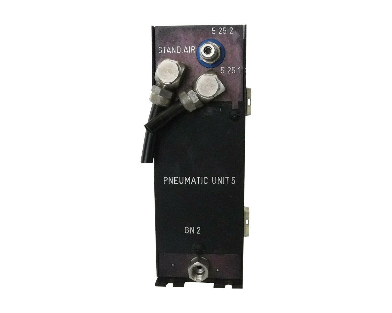
描述
产品简要说明
ASML PASS 25005000 280854845是ASML早期推出的模块化光刻系统,专为20世纪80年代至90年代的半导体制造设计。其核心功能包括:
电动晶圆台控制:支持4-12英寸晶圆处理,套准精度≤12nm(最新型号)。
多光源适配:兼容i线(365nm)、KrF(248nm)及ArF(193nm)准分子激光器。
模块化扩展:可根据工艺需求灵活选配扫描式/步进式光刻模块。
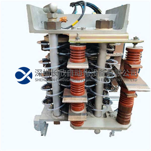
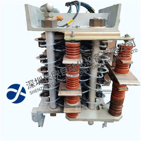
产品详细说明
1.技术架构与创新
电动化驱动系统:
晶圆台定位精度:±0.1μm(扫描模式),±0.05μm(步进模式)。
动态补偿技术:通过压电陶瓷驱动实现纳米级振动抑制。
多模态光源集成:
i线光源:波长365nm,支持0.7μm分辨率。
KrF光源:波长248nm,支持0.35μm分辨率。
模块化设计:
可扩展架构:通过独立模块(如扫描仪、步进仪、检测单元)实现功能叠加。
快速迭代能力:单台设备可适配不同工艺需求,降低产线改造成本。
2.工艺适配性
逻辑芯片制造:
关键层处理:支持0.5μm至0.35μm制程,套准精度≤100nm。
多层对准:采用双频激光干涉仪实现层间对准误差≤50nm。
存储器生产:
动态随机存取存储器(DRAM):支持64Mbit至256Mbit芯片量产。
非易失性存储器(NVM):兼容浮栅结构刻蚀工艺。
Product brief description
ASML PASS 25005000 280854845 is a modular lithography system launched by ASML in the early days,designed for semiconductor manufacturing from the 1980s to 1990s.Its core functions include:
Electric wafer table control:supports 4-12-inch wafer processing,registration accuracy≤12nm(latest model).
Multi-light source adaptation:compatible with i-line(365nm),KrF(248nm)and ArF(193nm)excimer lasers.
Modular expansion:Scanning/step lithography modules can be flexibly selected according to process requirements.
Product details
1.Technical Architecture and Innovation
Electrostatic drive system:
Wafer positioning accuracy:±0.1μm(scan mode),±0.05μm(step mode).
Dynamic compensation technology:nanoscale vibration suppression is achieved through piezoelectric ceramic driving.
Multimodal light source integration:
i-line light source:wavelength 365nm,supports 0.7μm resolution.
KrF light source:wavelength 248nm,supports 0.35μm resolution.
Modular design:
Scalable architecture:Functional overlay is achieved through independent modules(such as scanners,steppers,detection units).
Rapid iteration capability:Single equipment can adapt to different process requirements,reducing production line transformation costs.
2.Process adaptability
Logic chip manufacturing:
Key layer processing:Supports 0.5μm to 0.35μm process,registration accuracy≤100nm.
Multi-layer alignment:A dual-frequency laser interferometer is used to achieve an interlayer alignment error of≤50nm.
Memory production:
Dynamic Random Access Memory(DRAM):Supports mass production of 64Mbit to 256Mbit chips.
Nonvolatile memory(NVM):compatible with floating gate structure etching process.