描述
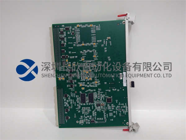
FORCE PMC234是一款高性能、低功耗的微型控制器,专为工业控制、自动化系统及精密测量设计。以下是其核心功能与技术特点的综合解析:
一、产品概述
架构:基于RISC架构的双处理单元(FPP)设计,支持并行处理与传统单片机模式切换,指令执行效率高(大部分为单周期指令)。
存储器:4K×16位OTP程序存储器,208字节数据存储器,支持可编程堆栈深度与灵活寻址模式。
模拟输入:11通道12位ADC,内置Band-gap参考电压(1.20V±0.03V),支持绝对电压测量与信号比较功能。
二、核心特性
高精度数据采集
支持11通道高精度ADC,其中1通道用于内部基准电压生成,适用于力传感器、温度等信号的精确测量。
内置硬件比较器,可实现信号电压快速比较与阈值判断。
低功耗设计
工作电压范围2.2V~5.5V,支持四种工作模式(正常、低速、绿色、休眠),休眠模式下功耗仅0.5μmailto:A 3.3V。
内置32kHz低频振荡器与16MHz高频RC振荡器,满足不同场景的功耗与性能需求。
丰富的外设接口
26个IO引脚:每引脚支持10mA驱动能力,可配置为唤醒源,支持按键扫描与LCD驱动功能。
时钟与定时器:16位硬件定时器(可作为RTC使用)、8位定时器(支持PWM输出),提供灵活的时间管理。
通信功能:支持I²C、SPI、UART等接口协议,方便扩展外部设备。
LCD显示支持
内置4×21点阵LCD驱动模块,可生成VDD/2偏置电压,降低外部硬件成本。
三、应用领域
工业自动化:机械臂、机器人控制、工业传感器监测。
消费电子:智能家电、电饭煲、电陶炉等需要精密控制的设备。
移动设备:手持仪器、便携式医疗设备(低功耗与宽电压特性适用)。
嵌入式系统:嵌入式控制器、数据采集终端。
四、技术优势
双处理单元协同:两个FPP单元可并行执行不同任务(如数据采集与逻辑控制),提升系统响应速度。
宽温与可靠性:工作温度范围-40℃~85℃,适用于工业环境;内置LVD(低电压检测)功能,支持8级复位阈值设定。
开发便捷性:独立的IO地址与存储空间,支持直接/间接寻址模式,降低代码开发复杂度。
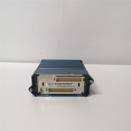
FORCE PMC234 is a high-performance,low-power microcontroller designed for industrial control,automation systems and precision measurement.The following is a comprehensive analysis of its core functions and technical features:
I.Product Overview
Architecture:Dual processing unit(FPP)design based on RISC architecture,supports parallel processing and traditional microcontroller mode switching,and has high instruction execution efficiency(mostly single-cycle instructions).
Memory:4K×16-bit OTP program memory,208-byte data memory,supports programmable stack depth and flexible addressing mode.
Analog input:11-channel 12-bit ADC,built-in Band-gap reference voltage(1.20V±0.03V),supports absolute voltage measurement and signal comparison functions.
II.Core Features
High-precision data acquisition
Supports 11-channel high-precision ADC,ofwhich 1 channel is used for internal reference voltage generation,suitable for accurate measurement of force sensors,temperature and other signals.
Built-in hardware comparator,which can realize fast signal voltage comparison and threshold judgment.
Low power design
The operating voltage range is 2.2V~5.5V,and it supports four working modes(normal,low speed,green,and sleep).The power consumption in sleep mode is only 0.5μmailto:A 3.3V.
Built-in 32kHz low-frequency oscillator and 16MHz high-frequency RC oscillator to meet the power consumption and performance requirements of different scenarios.
Rich peripheral interfaces
26 IO pins:Each pin supports 10mA driving capability,can be configured as a wake-up source,and supports key scanning and LCD driving functions.
Clock and timer:16-bit hardware timer(can be used as RTC),8-bit timer(supports PWM output),providing flexible time management.
Communication function:supports I²C,SPI,UART and other interface protocols,which is convenient for expanding external devices.
LCD display support
Built-in 4×21 dot matrix LCD driver module,which can generate VDD/2 bias voltage to reduce external hardware costs.
III.Application field
Industrial automation:robotic arm,robot control,industrial sensor monitoring.
Consumer electronics:smart home appliances,rice cookers,electric ceramic stoves and other equipment that require precision control.
Mobile devices:handheld instruments,portable medical devices(applicable to low power consumption and wide voltage characteristics).
Embedded systems:embedded controllers,data acquisition terminals.
IV.Technical advantages
Dual processing unit collaboration:two FPP units can perform different tasks in parallel(such as data acquisition and logic control),improving system response speed.
Wide temperature and reliability:The operating temperature range is-40℃~85℃,suitable for industrial environments;built-in LVD(low voltage detection)function,supporting 8-level reset threshold setting.
Development convenience:independent IO address and storage space,support direct/indirect addressing mode,reducing code development complexity.

