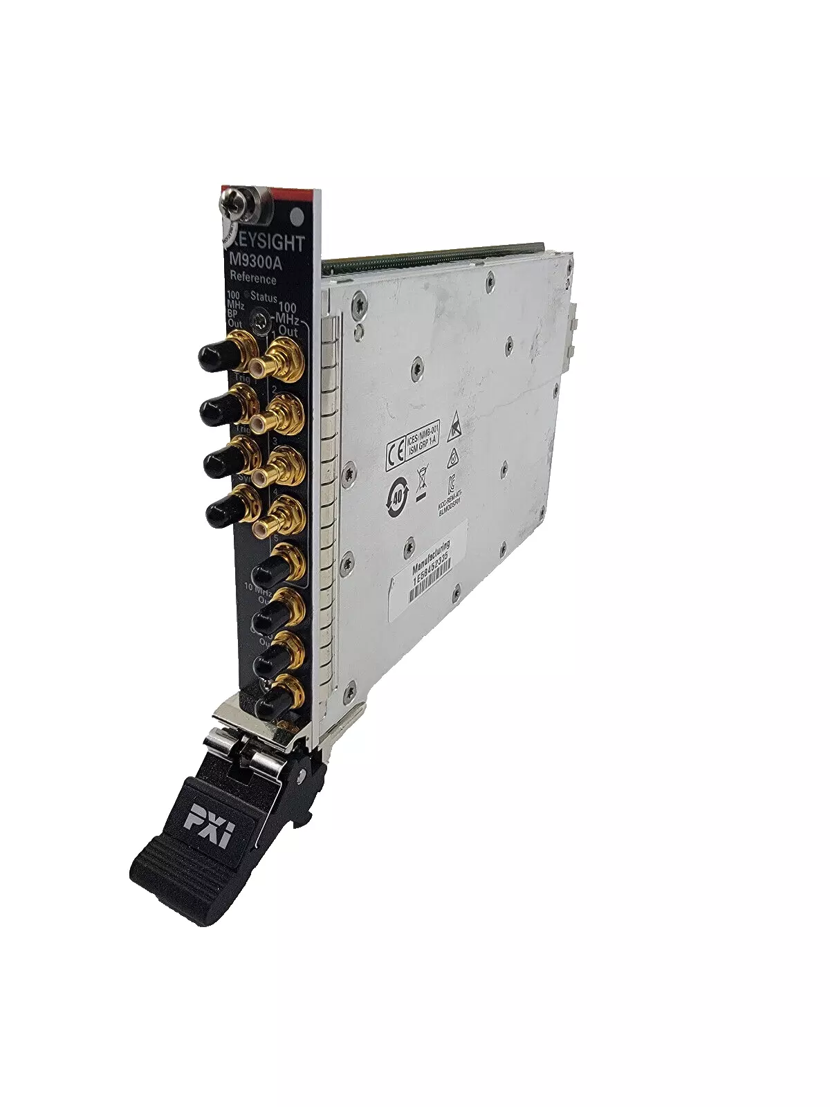
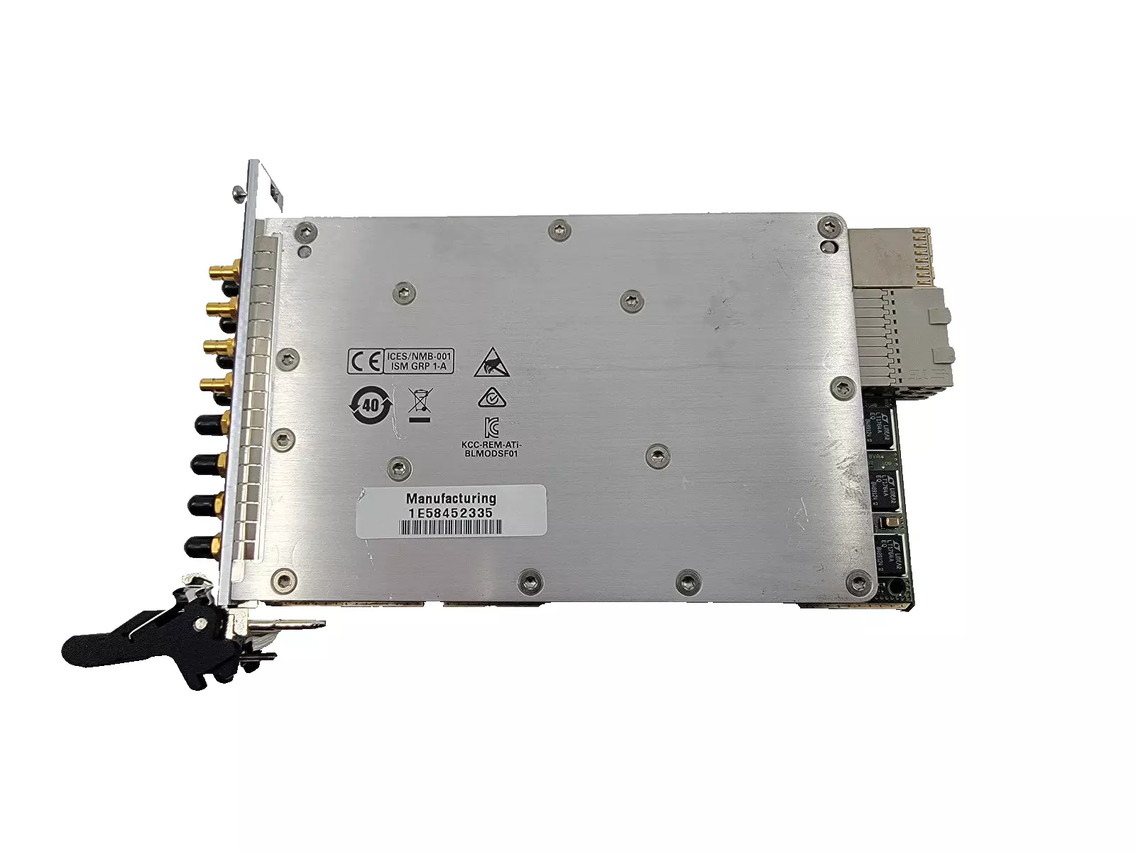
描述
产品定位与功能
NI M9300A推测为PXIe架构的高性能射频信号生成与分析模块,面向5G通信、雷达系统及国防电子测试场景。其核心功能包括:
矢量信号收发:支持调制/解调、频谱分析及实时信号处理;
宽频覆盖:频率范围可能覆盖DC至110 GHz(通过外接变频模块扩展);
多通道同步:支持多卡级联实现MIMO或分布式测试系统。
核心参数推测
射频性能
-中心频率:基带至26.5 GHz(内置混频器或外接模块扩展);
-带宽:瞬时带宽1 GHz(可选更高带宽型号);
-EVM(误差向量幅度):<0.5%(典型值,QPSK调制)。
数字信号处理(DSP)
-采样率:12 GS/s(ADC/DAC);
-存储深度:2 GB每通道(支持流式传输至PXIe存储);
-FPGA资源:内置Xilinx Kintex-7 FPGA(可自定义信号处理算法)。
接口与同步
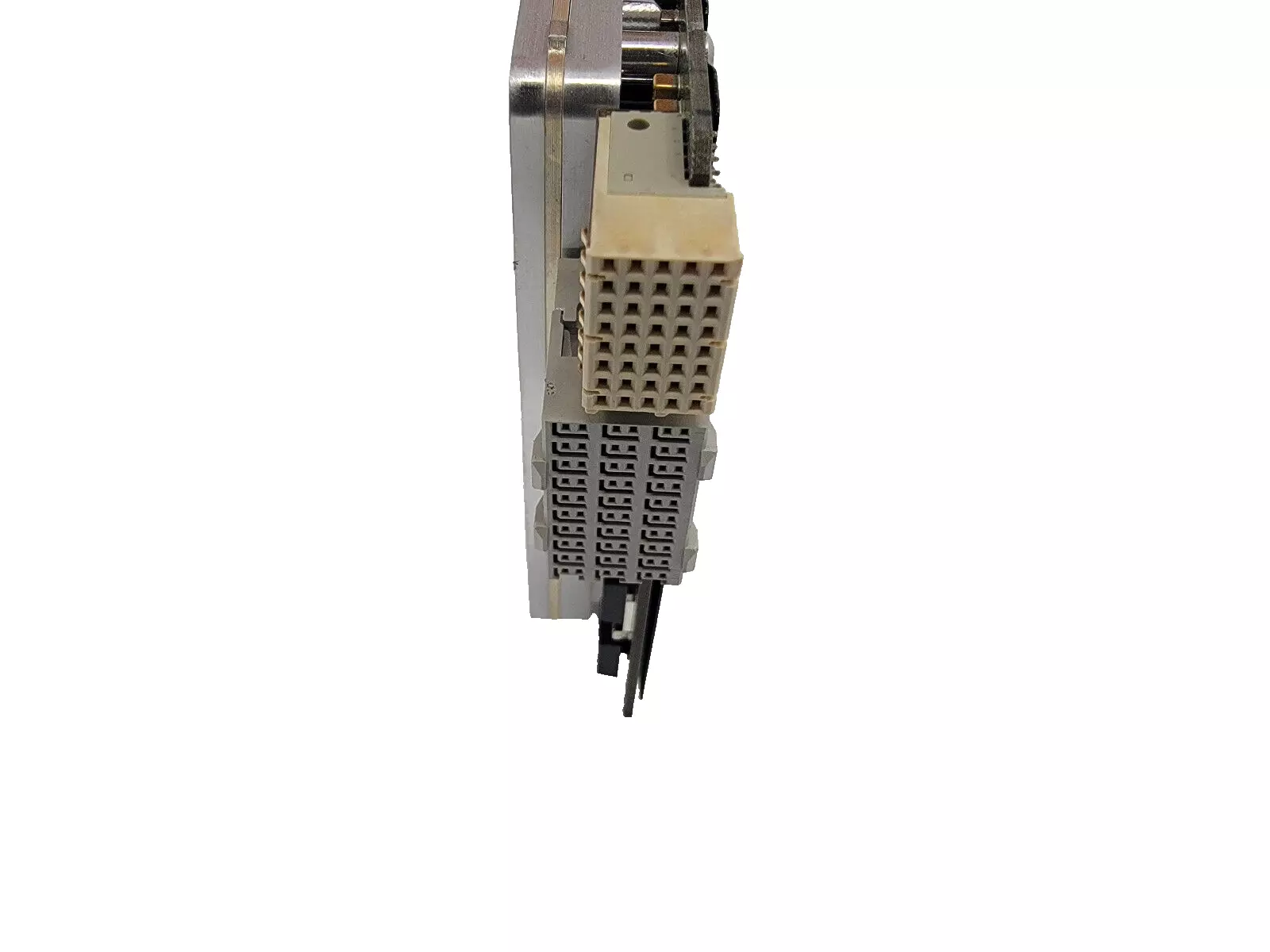
-PXIe总线:x4通道(4 GB/s传输速率);
-触发系统:支持10 MHz参考时钟、PXI星触发及外部GPIO同步。
技术特点
开放性架构
-软件定义:通过LabVIEW FPGA及NI-SCOPE驱动实现自定义协议解析;
-协议支持:预置5G NR、LTE、Wi-Fi 6E信号模型库。
环境适应性
-散热设计:强制风冷+热插拔模块化结构(符合PXIe 4U高度标准);
-振动耐受:符合MIL-STD-810G标准(适合车载或舰载测试部署)。
集成开发支持
-示波器功能:兼容传统数字磷迹显示(DPO)技术;
-AI辅助分析:可集成TensorFlow Lite模型进行实时信号分类。
典型应用场景
通信测试
-5G基站射频一致性测试(符合3GPP TS 38.141标准);
-卫星通信链路模拟(多普勒效应补偿)。
电子战仿真
-脉冲雷达信号生成(支持PRI捷变与脉内调制);
-欺骗干扰波形设计(时敏干扰模式)。
Product Positioning and Functions
The NI M9300A is speculated to be a high-performance RF signal generation and analysis module of the PXIe architecture,aiming at 5G communications,radar systems and defense electronic testing scenarios.Its core functions include:
Vector signal transmission and reception:supports modulation/demodulation,spectrum analysis and real-time signal processing;
Broadband coverage:The frequency range may cover DC to 110 GHz(extended via external frequency converter module);
Multi-channel synchronization:supports multi-card cascade implementation of MIMO or distributed testing systems.
Core parameter estimation
RF performance
-Center frequency:baseband to 26.5 GHz(built-in mixer or external module extension);
-Bandwidth:Instantaneous bandwidth 1 GHz(higher bandwidth models are available);
-EVM(Error vector amplitude):<0.5%(typical,QPSK modulation).
Digital Signal Processing(DSP)
-Sampling rate:12 GS/s(ADC/DAC);
-Storage depth:2 GB per channel(supports streaming to PXIe storage);
-FPGA resources:Built-in Xilinx Kintex-7 FPGA(customizable signal processing algorithm).
Interface and synchronization
-PXIe bus:x4 channel(4 GB/s transmission rate);
-Trigger system:Supports 10 MHz reference clock,PXI star trigger and external GPIO synchronization.
Technical Features
Open architecture
-Software definition:implement custom protocol analysis through LabVIEW FPGA and NI-SCOPE driver;
-Protocol support:pre-installed 5G NR,LTE,Wi-Fi 6E signal model library.
Environmental adaptability
-Heat dissipation design:forced air cooling+hot-swap modular structure(compliant with PXIe 4U height standard);
-Vibration resistance:Complies with MIL-STD-810G standard(suitable for on-board or ship-based testing deployment).
Integrated development support
-Oscilloscope functions:compatible with traditional digital phosphorus trace display(DPO)technology;
-AI-assisted analysis:The TensorFlow Lite model can be integrated for real-time signal classification.
Typical application scenarios
Communication test
-5G base station radio frequency consistency test(compliant with 3GPP TS 38.141 standard);
-Satellite communication link simulation(Doppler effect compensation).
Electronic warfare simulation
-Pulse radar signal generation(supports PRI agility and intrapulse modulation);
-Spoofing interference waveform design(time sensitive interference mode).