描述
一、基本参数
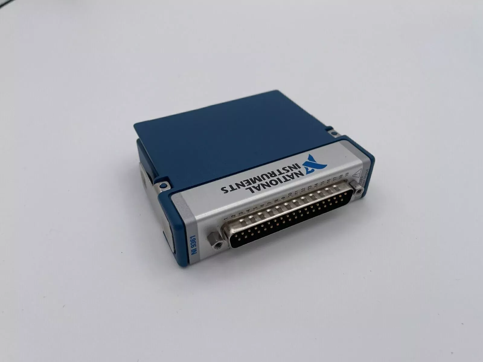
模块类型:
CompactRIO模块:兼容NI CompactRIO平台(cRIO-90xx系列机箱),支持实时(RT)和FPGA编程。
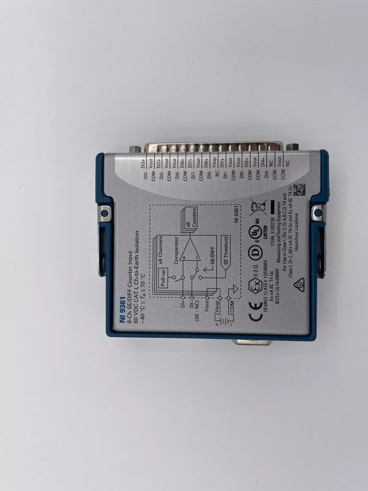
数字输入/输出(DIO):32通道双向数字I/O,可独立配置为输入或输出。
电气特性:
电压等级:
输入:兼容TTL(0-5 V)和LVDS(低压差分信号,350 mV差分)。
输出:支持TTL(0-5 V),最大驱动电流24 mA/通道。
输入阈值:
TTL模式:低电平≤0.8 V,高电平≥2.0 V。
LVDS模式:差分输入范围±1.4 V(典型值)。
隔离:
通道-地隔离:每通道300 Vrms隔离,防止共模电压干扰。
通道间隔离:无(需通过外部光耦或数字隔离器实现)。
时序与速度:
最大时钟频率:40 MHz(FPGA可编程时钟)。
输入延迟:<50 ns(从信号边沿到FPGA捕获)。
输出延迟:<30 ns(从FPGA更新到输出信号稳定)。
物理特性:
尺寸:CompactRIO标准模块尺寸(3U,单槽宽度)。
连接器:40针C Series连接器,支持NI标准接线端子(如TB-4300)。
二、核心功能
高速数字信号处理:
FPGA集成:可直接在FPGA上实现自定义数字逻辑(如编码器解码、PWM生成、脉冲计数)。
实时(RT)支持:通过LabVIEW Real-Time模块实现确定性控制与数据记录。
同步采样:支持CompactRIO背板时钟同步,实现多模块微秒级同步操作。
灵活的配置模式:
静态I/O:通过RT程序配置固定输入/输出方向。
动态重配置:在FPGA中实时切换通道方向(如双向总线控制)。
特殊功能:
脉冲宽度调制(PWM):生成可变占空比信号(需FPGA编程)。
四倍频编码器接口:支持A/B/Z相编码器信号解码。
事件计数器:对输入脉冲进行上升沿/下降沿计数。
硬件触发与中断:
触发输入:支持外部TTL信号触发FPGA逻辑或RT任务。
中断生成:输入信号边沿可触发RT程序中断,实现快速响应。
三、典型应用场景
工业自动化与控制:
PLC替代方案:通过FPGA实现高速数字逻辑控制(如运动控制、安全系统)。
传感器接口:连接数字传感器(如光电开关、限位开关、编码器)。
机器人与运动控制:
伺服驱动器控制:生成PWM信号驱动步进电机或伺服电机。
多轴同步:通过FPGA实现多轴编码器信号同步采集与处理。
硬件在环(HIL)测试:
模拟数字传感器:输出数字信号模拟ECU输入(如CAN总线故障注入)。
实时故障注入:通过FPGA动态修改数字信号状态,测试系统容错能力。
通信与协议测试:
SPI/I²C主机模拟:在FPGA中实现自定义总线协议。
数字信号分析:采集高速数字信号(如UART、曼彻斯特编码)进行协议解析。
四、优势与局限性
优势:
高速与低延迟:40 MHz FPGA时钟+<50 ns输入延迟,适合实时控制。
高通道密度:单模块32通道,减少机箱插槽占用。
灵活性极强:FPGA可编程性支持任意数字逻辑实现。
局限性:
无模拟功能:若需混合信号采集,需搭配其他模块(如NI-9215)。
LVDS输入需外部匹配:LVDS模式需外部终端电阻(100Ω差分)。
成本较高:相比非隔离DIO模块(如NI-9401),价格更高。
1.Basic parameters
Module type:
CompactRIO module:compatible with NI CompactRIO platform(cRIO-90xx series chassis),supports real-time(RT)and FPGA programming.
Digital input/output(DIO):32 channels of bidirectional digital I/O,independently configurable as input or output.
Electrical characteristics:
Voltage level:
Input:compatible with TTL(0-5 V)and LVDS(low voltage differential signal,350 mV differential).
Output:supports TTL(0-5 V),maximum drive current 24 mA/channel.
Input threshold:
TTL mode:low level≤0.8 V,high level≥2.0 V.
LVDS mode:differential input range±1.4 V(typical).
Isolation:
Channel-ground isolation:300 Vrms isolation per channel to prevent common-mode voltage interference.
Channel-to-channel isolation:None(needs to be implemented through external optocouplers or digital isolators).
Timing and speed:
Maximum clock frequency:40 MHz(FPGA programmable clock).
Input delay:<50 ns(from signal edge to FPGA capture).
Output delay:<30 ns(from FPGA update to output signal stability).
Physical characteristics:
Size:CompactRIO standard module size(3U,single slot width).
Connector:40-pin C Series connector,supports NI standard terminal blocks(such as TB-4300).
2.Core functions
High-speed digital signal processing:
FPGA integration:Custom digital logic(such as encoder decoding,PWM generation,pulse counting)can be implemented directly on the FPGA.
Real-time(RT)support:Deterministic control and data logging through the LabVIEW Real-Time module.
Synchronous sampling:Supports CompactRIO backplane clock synchronization to achieve microsecond-level synchronous operation of multiple modules.
Flexible configuration mode:
Static I/O:Configure fixed input/output direction through RT program.
Dynamic reconfiguration:Switch channel direction in real time in FPGA(such as bidirectional bus control).
Special functions:
Pulse width modulation(PWM):Generate variable duty cycle signal(FPGA programming required).
Quadruple frequency encoder interface:Support A/B/Z phase encoder signal decoding.
Event counter:Count the rising/falling edge of input pulses.
Hardware trigger and interrupt:
Trigger input:Support external TTL signal to trigger FPGA logic or RT task.
Interrupt generation:Input signal edge can trigger RT program interrupt for fast response.
III.Typical application scenarios
Industrial automation and control:
PLC alternative:Implement high-speed digital logic control(such as motion control,safety system)through FPGA.
Sensor interface:Connect digital sensors(such as photoelectric switches,limit switches,encoders).
Robotics and motion control:
Servo drive control:Generate PWM signals to drive stepper motors or servo motors.
Multi-axis synchronization:synchronous acquisition and processing of multi-axis encoder signals through FPGA.
Hardware-in-the-loop(HIL)testing:
Analog digital sensors:output digital signals to simulate ECU inputs(such as CAN bus fault injection).
Real-time fault injection:dynamically modify digital signal states through FPGA to test system fault tolerance.
Communication and protocol testing:
SPI/I²C host simulation:implement custom bus protocols in FPGA.
Digital signal analysis:collect high-speed digital signals(such as UART,Manchester encoding)for protocol analysis.
IV.Advantages and limitations
Advantages:
High speed and low latency:40 MHz FPGA clock+<50 ns input latency,suitable for real-time control.
High channel density:32 channels per module,reducing chassis slot occupancy.
Extremely flexible:FPGA programmability supports arbitrary digital logic implementation.
Limitations:
No analog function:If mixed signal acquisition is required,other modules(such as NI-9215)are required.
LVDS inputs require external termination:LVDS mode requires external termination resistors(100Ωdifferential).
Higher cost:More expensive than non-isolated DIO modules(such as NI-9401).