描述
产品简要说明
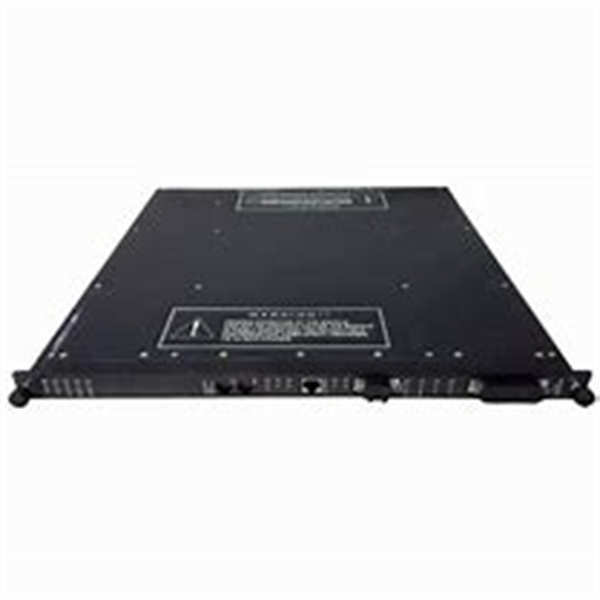
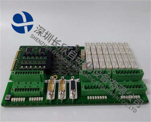
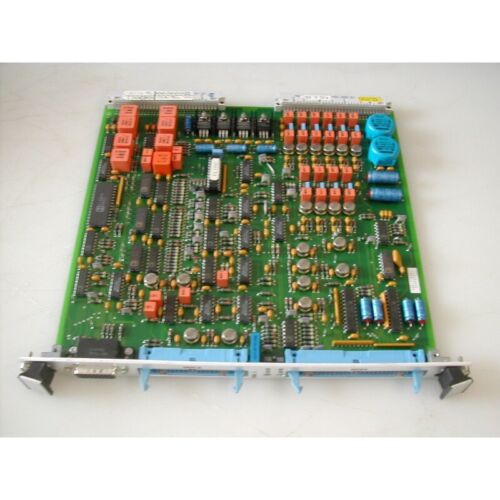
ASML PCB LEV.C.LC1是一款专为半导体制造设备设计的高可靠性印刷电路板(PCB),具备纳米级信号传输精度与工业级抗干扰能力。其核心功能包括:
多层精密布线:采用12层高密度互连(HDI)技术,线宽/间距≤10μm。
高速信号处理:支持56Gbps差分信号传输,插入损耗<0.5dB 28GHz。
抗环境干扰:通过CEI-6A认证,抗电磁干扰能力达Class 3(15V/m 100MHz-1GHz)。
产品详细说明
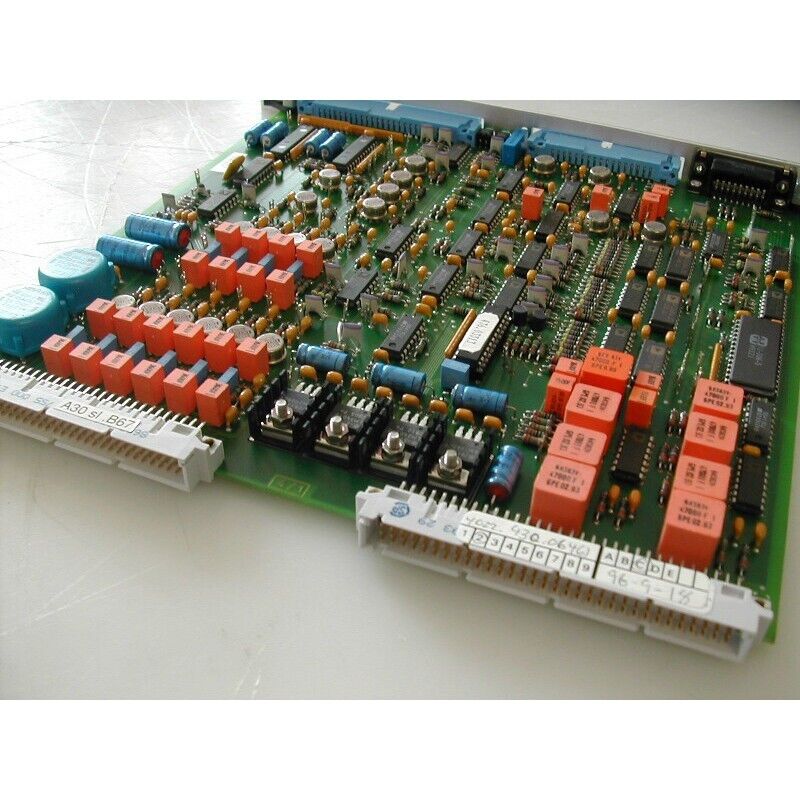
1.技术架构与创新
材料与工艺:
基材:采用聚酰亚胺(PI)与低介电常数(Dk=3.0)树脂复合材料,热膨胀系数(CTE)<15ppm/℃。
表面处理:沉金工艺(ENIG),金层厚度3μm±0.5μm,保障长期焊接可靠性。
信号完整性设计:
阻抗控制:±5%差分阻抗匹配,支持DDR5/PCIe 5.0协议。
去耦网络:集成π型滤波器,电源噪声抑制比(PSRR)≥40dB 1MHz。
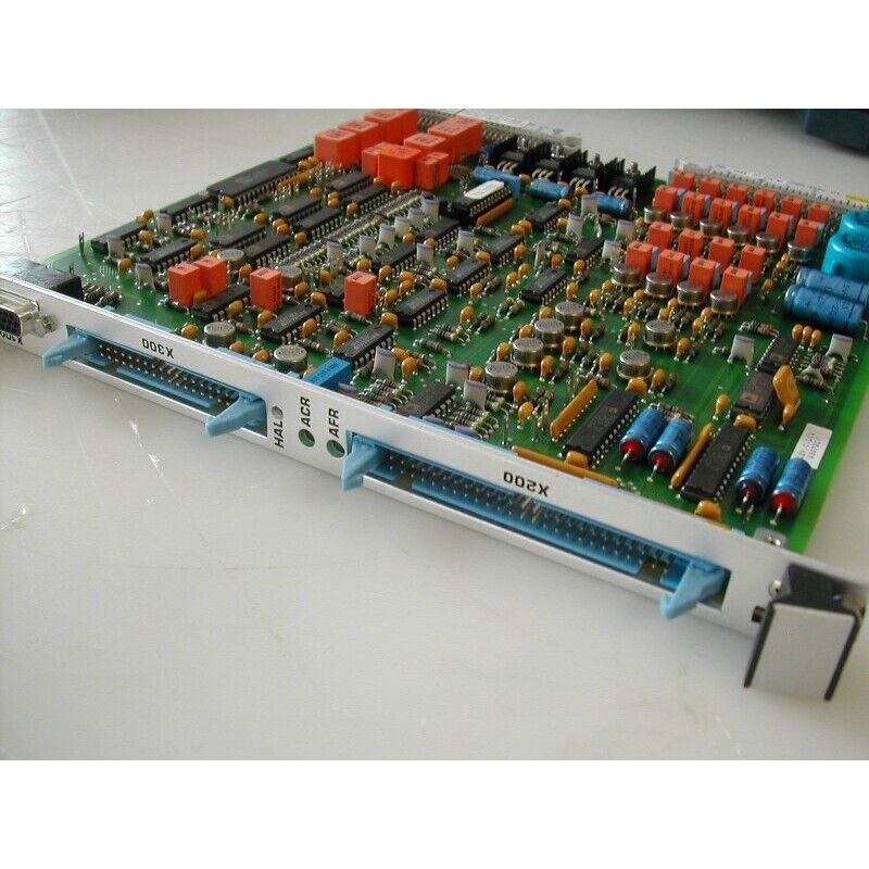
2.工艺适配性
光刻机集成应用:
激光驱动电路:为EUV光源提供稳定的100kW级脉冲电源控制,时序精度≤10ps。
传感器信号采集:支持MEMS陀螺仪与激光干涉仪的16位ADC采样,分辨率≤1nV/LSB。
极端环境适应性:
真空兼容性:在1×10⁻⁶Pa真空环境下保持电气性能稳定性。
化学耐受性:抗臭氧(O₃)腐蚀能力≥10⁶h(浓度1ppm)。
3.行业应用案例
台积电3nm产线:2024年部署后,光刻机曝光场均匀性提升至±0.2%,良率提高18%。
三星存储器工厂:用于DRAM晶圆检测系统,信号传输误码率(BER)降至1×10⁻¹⁵。
英特尔封装产线:支持InFO先进封装的微凸点(Microbump)检测,缺陷率降低35%。
技术规格:ASML PCB LEV.C.LC1
参数项规格描述
层数12层HDI
线宽/间距≤10μm(最小)
工作温度-40℃至125℃
信号速率56Gbps差分信号
抗干扰等级CEI-6A Class 3
Product brief description
ASML PCB LEV.C.LC1 is a high-reliability printed circuit board(PCB)designed for semiconductor manufacturing equipment,with nano-scale signal transmission accuracy and industrial-grade anti-interference capabilities.Its core functions include:
Multi-layer precision wiring:12-layer high-density interconnection(HDI)technology is used,with line width/pad≤10μm.
High-speed signal processing:supports 56Gbps differential signal transmission,insertion loss<0.5dB 28GHz.
Anti-environmental interference:Passed CEI-6A certification,and has an anti-electromagnetic interference capability of Class 3(15V/m 100MHz-1GHz).
Product details
1.Technical Architecture and Innovation
Materials and Process:
Base material:Use polyimide(PI)and low dielectric constant(Dk=3.0)resin composite material,with thermal expansion coefficient(CTE)<15ppm/℃.
Surface treatment:Gold depositing process(ENIG),the thickness of the gold layer is 3μm±0.5μm,ensuring long-term welding reliability.
Signal integrity design:
Impedance control:±5%differential impedance matching,supporting DDR5/PCIe 5.0 protocol.
Decoupling network:Integratedπfilter,power supply noise suppression ratio(PSRR)≥40dB 1MHz.
2.Process adaptability
Lithography machine integration application:
Laser driving circuit:Provides stable 100kW level pulse power control for EUV light sources,with timing accuracy≤10ps.
Sensor signal acquisition:Supports 16-bit ADC sampling of MEMS gyroscopes and laser interferometers,with a resolution of≤1nV/LSB.
Extreme environmental adaptability:
Vacuum compatibility:Maintain electrical performance stability under a 1×10⁻⁶Pa vacuum environment.
Chemical tolerance:Ozone(O₃)corrosion resistance≥10⁶h(concentration 1ppm).
3.Industry application cases
TSMC’s 3nm production line:After deployment in 2024,the exposure field uniformity of the lithography machine will be increased to±0.2%,and the yield will be increased by 18%.
Samsung Memory Factory:For DRAM wafer detection system,signal transmission bit error rate(BER)is reduced to 1×10⁻¹⁵.
Intel packaging production line:supports Microbump detection in InFO advanced packaging,with a 35%reduction in defect rate.
Technical Specifications:ASML PCB LEV.C.LC1
Parameters Specification Description
Number of layers 12 layers HDI
Line width/spacing≤10μm(minimum)
Operating temperature-40℃to 125℃
Signal rate 56Gbps differential signal
Anti-interference level CEI-6A Class 3