描述
一、产品概述
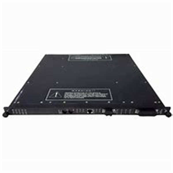
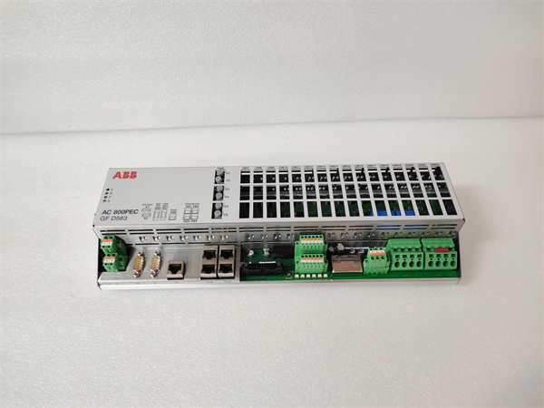
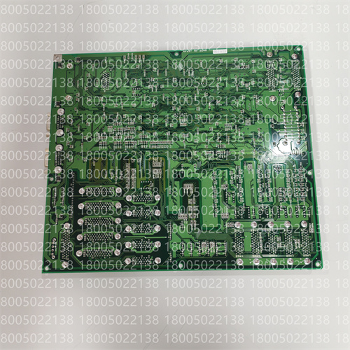
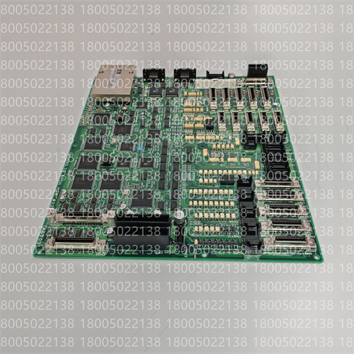
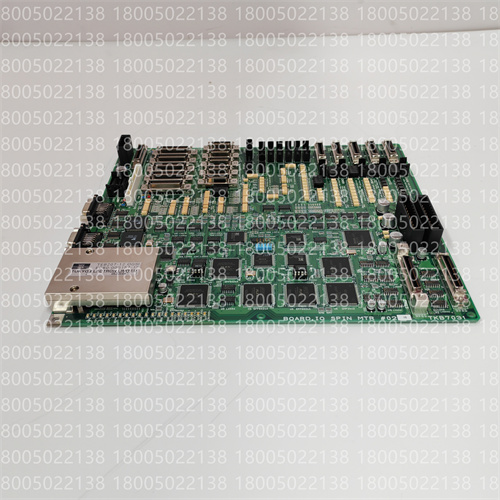
TEB207-12 OGSI EC80-000157-12是东京电子(Tokyo Electron Ltd.,TEL)推出的专用电子模块组件,主要用于半导体制造设备的核心控制子系统。该模块属于定制化设计,适用于真空蚀刻机、化学气相沉积(CVD)系统、物理气相沉积(PVD)设备及清洗机等场景。
二、核心功能与技术特性
功能定位
-推测用途:根据型号命名及行业经验,该模块可能承担以下功能之一:
-电源控制:调节设备供电稳定性,支持等离子体生成或真空系统运行;
-信号处理:负责工艺参数(如温度、压力)的采集与信号驱动;
-IO接口管理:协调设备与上层控制系统(如PLC/DCS)的数据交互。
技术参数
-兼容平台:TEL Unity、Trias、Eagle等系列半导体设备;
-接口类型:可能集成RF匹配器控制、腔体状态监测等专用接口;
-环境适应性:工业级设计,支持半导体制造所需的高精度与抗干扰需求。
三、典型应用场景
半导体制造
-蚀刻设备:参与等离子源功率调节,确保蚀刻均匀性;
-CVD/PVD系统:监控气体流量、腔体真空度等关键参数。
维护与升级
-作为TEL设备的替换模块,用于故障修复或系统性能优化;
-支持与新型控制协议(如OPC UA)的集成,适配智能化产线改造。
1.Product Overview
TEB207-12 OGSI EC80-000157-12 is a dedicated electronic module component launched by Tokyo Electron Ltd.,which is mainly used for the core control subsystem of semiconductor manufacturing equipment.This module is a customized design and is suitable for vacuum etching machines,chemical vapor deposition(CVD)systems,physical vapor deposition(PVD)equipment and cleaning machines.
2.Core functions and technical characteristics
Functional positioning
-Speculative purpose:According to model naming and industry experience,this module may undertake one of the following functions:
-Power control:adjusts the power supply stability of the equipment and supports plasma generation or vacuum system operation;
-Signal processing:Responsible for the acquisition and signal driving of process parameters(such as temperature and pressure);
-IO interface management:coordinates the data interaction between the equipment and the upper control system(such as PLC/DCS).
Technical parameters
-Compatible platform:TEL Unity,Trias,Eagle and other series of semiconductor devices;
-Interface type:It may integrate dedicated interfaces such as RF matcher control,cavity status monitoring,etc.;
-Environmental adaptability:Industrial-grade design that supports the high precision and anti-interference requirements required for semiconductor manufacturing.
3.Typical application scenarios
Semiconductor manufacturing
-Etching equipment:participate in plasma source power regulation to ensure etching uniformity;
-CVD/PVD system:Monitor key parameters such as gas flow rate,cavity vacuum degree,etc.
Maintenance and Upgrade
-As a replacement module for TEL equipment,used for fault repair or system performance optimization;
-Supports integration with new control protocols(such as OPC UA)and adapts to intelligent production line transformation.